Analog HfOx/HfOy homojunction memristor and regulation and control method thereof

A technology of homojunction and memristor, which is applied in the field of analog HfOx/HfOy homojunction memristor and its regulation, can solve the problems of small analog resistive switching window, working speed, insufficient cycle characteristics of devices, etc., and achieve electric field The effect of large voltage division, high resistance and low resistance

Active Publication Date: 2020-03-24
HUAZHONG UNIV OF SCI & TECH
View PDF12 Cites 7 Cited by
  • Summary
  • Abstract
  • Description
  • Claims
  • Application Information

AI Technical Summary

Problems solved by technology

[0006] Yang Yuchao of Peking University and others (a linear slow-change memristor and its preparation method, CN106098932A) disclose a linear slow-change memristor and its preparation method. Its principle is to insert a A diffusion modulation layer that has a modulation effect on the ion diffusion rate can achieve different modulation effects, and optimize the characteristics...

Method used


Image

  • Analog HfOx/HfOy homojunction memristor and regulation and control method thereof
  • Analog HfOx/HfOy homojunction memristor and regulation and control method thereof
  • Analog HfOx/HfOy homojunction memristor and regulation and control method thereof

Examples


Embodiment 1

[0061] Embodiment 1: A kind of large window simulation type HfO x Preparation method of homojunction memristor

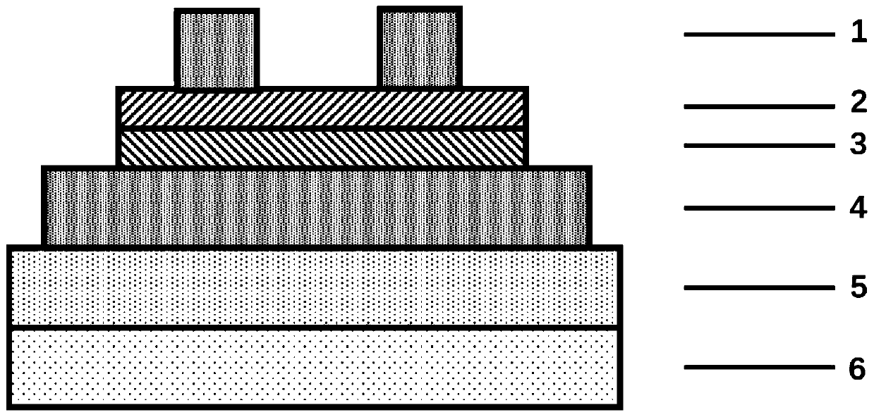
[0062] The HfO provided by embodiment 1 x Memristor, Pt / HfO with small square structure y / HfO x / Ti memristor, whose structure is as figure 1 , Figure 7 shown; wherein, the bottom electrode is Ti with a thickness of 100nm, and the functional layer is HfO with a thickness of 10nm x and 4nm HfO y , x=1.72, y=1.93; the upper electrode is Pt with a thickness of 100nm.

[0063] The following specifically sets forth the embodiment HfO x The preparation method of memristor; Concrete steps are as follows:

[0064] (1) The first step: prepare the lower electrode:

[0065] Sputtering: In long SiO 2 The lower electrode Ti with a thickness of 100nm was prepared on the Si substrate of the insulating layer by magnetron sputtering; the sputtering process conditions were: background vacuum 5*10 -5 Pa, the working pressure is 0.5Pa, the DC sputtering power is 100W, and ...

Embodiment 2

[0075] Embodiment 2: A kind of large window simulation type HfO x Regulation and testing method of homojunction memristor

[0076] The following is a method for regulating and testing the memristor prepared in Example 1, which specifically includes the following steps:

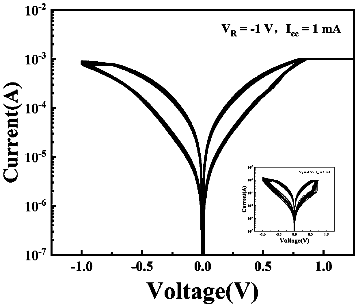
[0077] (1) The memristor units in the first row and the first column of the small square array structure memristor are pre-formed conductive channels; the scanning voltage used for forward I / V voltage scanning is 5V, and the current limit is 300μA.

[0078] (2) Perform 20 bidirectional I / V voltage scans on the memristor unit until stable RESET, SET voltage values ​​and their corresponding high and low resistance states appear in the memristor unit;

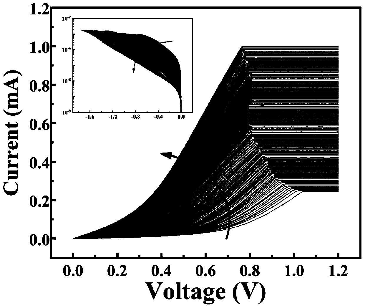
[0079] (3) Perform a DC gradient test on the memristor unit, using continuous unidirectional SET / RESET voltage to scan; the initial low resistance is 2.6kΩ, the SET voltage amplitude is 1.2V, and the limiting current is from 240μA to 1mA, with a step size is 5µ...

Embodiment 3

[0097] Embodiment 3: A kind of large window simulation type HfO x Preparation method of homojunction memristor

[0098] The HfO provided by embodiment 3 x Memristor, Pt / HfO with small square structure y / HfO x / Ti memristor, whose structure is as figure 1 shown; wherein, the bottom electrode is Ti with a thickness of 100nm, and the functional layer is HfO with a thickness of 10nm x and 4nm HfO y , x=1.6, y=1.93; the upper electrode is Pt with a thickness of 100nm. The preparation process is the same as in Example 1.

[0099] Among them, the difference from Example 1 is that in the sputtering process, the first 10nm HfO x Oxygen storage layer, regrown 4nm HfO y Migration barrier layer; the process conditions of sputtering are: the background vacuum is 5*10 -3 Pa, working pressure are 0.67Pa, DC sputtering power is 100W, sputtering time is 306s, 120s respectively, Ar and O 2 The volume ratio is 38:9, 31:16;

[0100] When x=1.6, the corresponding HfO x There are more ...


PUM

PropertyMeasurementUnit
Thicknessaaaaaaaaaa
Thicknessaaaaaaaaaa
Thicknessaaaaaaaaaa

Abstract

The invention belongs to the technical field of microelectronic devices. The invention discloses an analog HfOx/HfOy homojunction memristor and a regulation and control method thereof. The homojunction memristor comprises a lower electrode layer, a functional layer and an upper electrode layer which are sequentially stacked from bottom to top, and the functional layer is an HfOx/HfOy homojunctionfunctional layer formed by stacking an HfOx layer and an HfOy layer from bottom to top; for the HfOx/HfOy homojunction functional layer, 1.6<x<1.8, 1.9<y<2, and the thickness of the HfOx layer is larger than that of the HfOy layer. According to the invention, the key device structure, especially the functional layer composition and the like, is improved; the hafnium oxide lamination with high/lowoxygen vacancies grown in a stacked manner is used as the resistive function layer, and compared with the prior art, the technical problems of small resistance gradual change window, low operation speed and poor consistency of an analog memristor and an electronic synaptic bionic device based on the analog memristor can be effectively solved.

Description

technical field [0001] The invention belongs to the technical field of microelectronic devices, and more specifically relates to an analog HfO x / HfO y A homojunction memristor and a control method thereof, the memristor can realize the gradual change control of the resistance value in the range of 2kΩ-200kΩ, has a large gradient window, and can be used as an electrical synaptic device in neuromorphic computing. Background technique [0002] Memristor is a connection including resistance, inductance and capacitance proposed by Professor Cai Shaotang and q are the fourth basic passive circuit elements. Due to its simple structure, low power consumption, high speed, and good compatibility with CMOS technology, memristors are widely used in storage, logic operations, and neural network computing. [0003] According to the difference between the resistance state and the resistive switching behavior of the memristor under the electrical signal, the memristor is further divide...

Claims


Application Information

Patent Timeline
IPC IPC(8): H01L45/00H01L21/66G11C29/50G11C13/00
CPCH01L22/14H01L22/20G11C13/004G11C29/50G11C2029/5004H10N70/245H10N70/026H10N70/8833
Inventor 孙华军田宝毅缪向水
Owner HUAZHONG UNIV OF SCI & TECH
Why Eureka
Try Eureka