High-concentration multi-junction solar cell and preparation method thereof

A technology for solar cells and high concentration of light, which is applied in photovoltaic power generation, circuits, electrical components, etc., and can solve problems such as large open circuit voltage and short circuit current, reduced battery conversion efficiency, and affecting battery fill factor

Inactive Publication Date: 2011-11-16
XIAMEN SANAN OPTOELECTRONICS TECH CO LTD
View PDF5 Cites 7 Cited by
  • Summary
  • Abstract
  • Description
  • Claims
  • Application Information

AI Technical Summary

Problems solved by technology

This type of battery can concentrate and focus hundreds of times of solar energy to a small battery chip to generate electricity through a concentrating lens, thereby saving solar cell chips on a large scale, but a higher concentration factor (~1000X) can make While the concentrating cell obtains a large open circuit voltage and short circuit current, it will also cause a larger series resistance of the cell, which seriously affects the fill factor of the cell and reduces the conversion efficiency of the cell.

Method used


Image

  • High-concentration multi-junction solar cell and preparation method thereof
  • High-concentration multi-junction solar cell and preparation method thereof

Examples


Embodiment 1

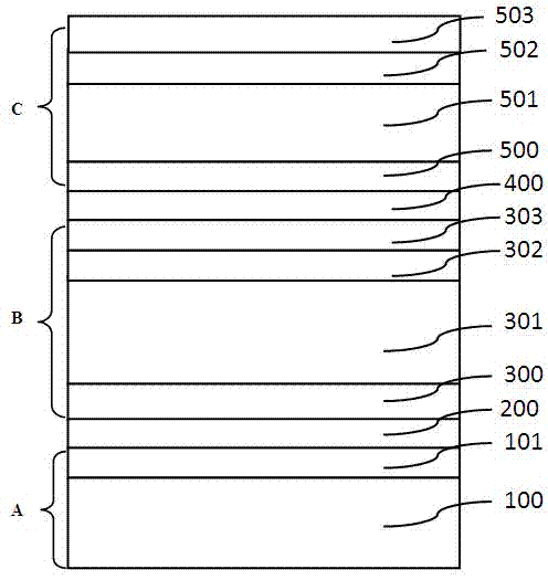
[0037] Such as figure 1 As shown, a high concentration multi-junction solar cell includes a Ge bottom cell A, a middle cell B, a top cell C and two tunnel junctions 200 and 400 therebetween.

[0038] More specifically, the figure shows: a p-type Ge substrate 100 on which an n-type Ga 0.5 In 0.5 The P window layer 101 constitutes the Ge bottom cell A.

[0039] A series of heavily doped p-type and n-type layers are deposited on top of the Ge bottom cell A to form a GaAs tunnel junction 200 for connecting the Ge bottom cell A to the middle cell B.

[0040] A mid-cell back field layer 300 for reducing recombination loss is deposited on top of the GaAs tunneling junction 200, and this layer is preferably made of p-type AlGaAs.

[0041] On the back field layer 300 of the middle cell, a base region 301 of the middle cell and an emitter layer 302 of the middle cell are deposited. In this preferred example, the base region 301 of the middle cell is made of p-type (In) GaAs, and its...

Embodiment 2

[0046] This embodiment is a preparation process of a high-power concentrating multi-junction solar cell described in Example 1, which includes the formation process of sub-cells A, B, C and layers between the sub-cells. In the MOCVD epitaxial growth process, the doping concentration of the emission layer can be gradually changed by adjusting the flow ratio of the n-type doping source in the reaction source.

[0047] Concrete preparation process comprises the following steps:

[0048] A p-type doped single crystal germanium substrate 100 with a thickness of 150 microns is used as the base region of the Ge bottom cell.

[0049] Clean the p-type Ge substrate 100 and put it into the MOCVD reaction chamber, first bake it at 750°C for 10 minutes, then lower the temperature to 600°C, and epitaxially grow n-type Ga 0.5 In 0.5 The P window layer 101 forms a Ge bottom cell A.

[0050] The GaAs tunneling junction 200 of the mid-bottom cell is epitaxially grown on the Ge bottom cell. ...


PUM


Abstract

The invention discloses a high-concentration multi-junction solar cell and a preparation method thereof. The high-concentration multi-junction solar cell consists of a top cell, a middle cell, a bottom cell and two tunneling junctions, wherein emission layers of the top cell and the middle cell adopt gradient doping layers; the emission layer of the top cell is hundreds of nanometers thicker than the conventional multi-junction cell. The invention relates to a high-concentration multi-junction solar cell, wherein emission layers of sub-cells on the top and middle parts respectively utilize the gradient doping manner, have higher open-circuit voltage and short-circuit current. Simultaneously, under the high-concentration condition, the emission layer of the top cell is thicker than the conventional multi-junction cell so that the whole serial resistance of the multi-junction cell is reduced, the filling factor of the cell is improved and the higher photoelectric conversion efficiency is achieved.

Description

technical field [0001] The invention belongs to the field of compound semiconductor solar cells, and in particular relates to a high-power concentrating multi-junction solar cell structure and a preparation method thereof. Background technique [0002] Photovoltaic power generation has experienced the development of the first generation of crystalline silicon cells and the second generation of thin film cells, and is currently entering the third generation of concentrated photovoltaic (CPV) technology. The core of CPV technology is the III-V concentrating multi-junction solar cell. Compared with other types of solar cells, the concentrating multi-junction solar cell has the advantages of high photoelectric conversion efficiency, good temperature characteristics, and short energy recovery cycle. Maximize the use of solar energy resources and reduce the damage to the environment caused by the construction of power stations. [0003] Multi-junction solar cells are composed of ...

Claims


Application Information

Patent Timeline
Patent Type & Authority Applications(China)
IPC IPC(8): H01L31/0352H01L31/06H01L31/18
CPCH01L31/0687Y02E10/544H01L31/076Y02E10/50Y02E10/548H01L31/0725Y02P70/50
Inventor 宋明辉林桂江吴志浩王良均刘建庆毕京锋熊伟平林志东
Owner XIAMEN SANAN OPTOELECTRONICS TECH CO LTD
Why Eureka
Try Eureka