System-in-package with fan-out WLCSP

a technology of fan-out and system-in-package, which is applied in the field of flip-chip packaging, can solve the problems high cost of high-performance fcbga package, and high cost of high-performance fcbga package, and achieve the effect of cost-effective and overcome the limitation of bump pitch on the substra

Active Publication Date: 2012-01-10
MEDIATEK INC
View PDF41 Cites 47 Cited by
  • Summary
  • Abstract
  • Description
  • Claims
  • Application Information

AI Technical Summary

Benefits of technology

[0010]It is one object of this invention to provide a flip-chip package for high-pin-count applications, which is cost-effective and can overcome the bump pitch limitation on the substrate.

Problems solved by technology

However, the conventional flip-chip technique is facing the challenge of bump pitch limitation on the substrate.
Besides, a high-performance FCBGA package is costly due to the expensive chip carrier substrate that typically comprises 1+2+1 or more-layer build up.
The bottleneck of the flip-chip roadmap is the bump pitch of the substrate since the development and shrinkage of the bump pitch is much slower than the die shrinking and the increase of the pin count.
To conquer the issue of such technology gap, Silicon interposer and TSV (Through Silicon Via) technology are the only and very expensive solution.

Method used


Image

  • System-in-package with fan-out WLCSP
  • System-in-package with fan-out WLCSP
  • System-in-package with fan-out WLCSP

Examples


Embodiment Construction

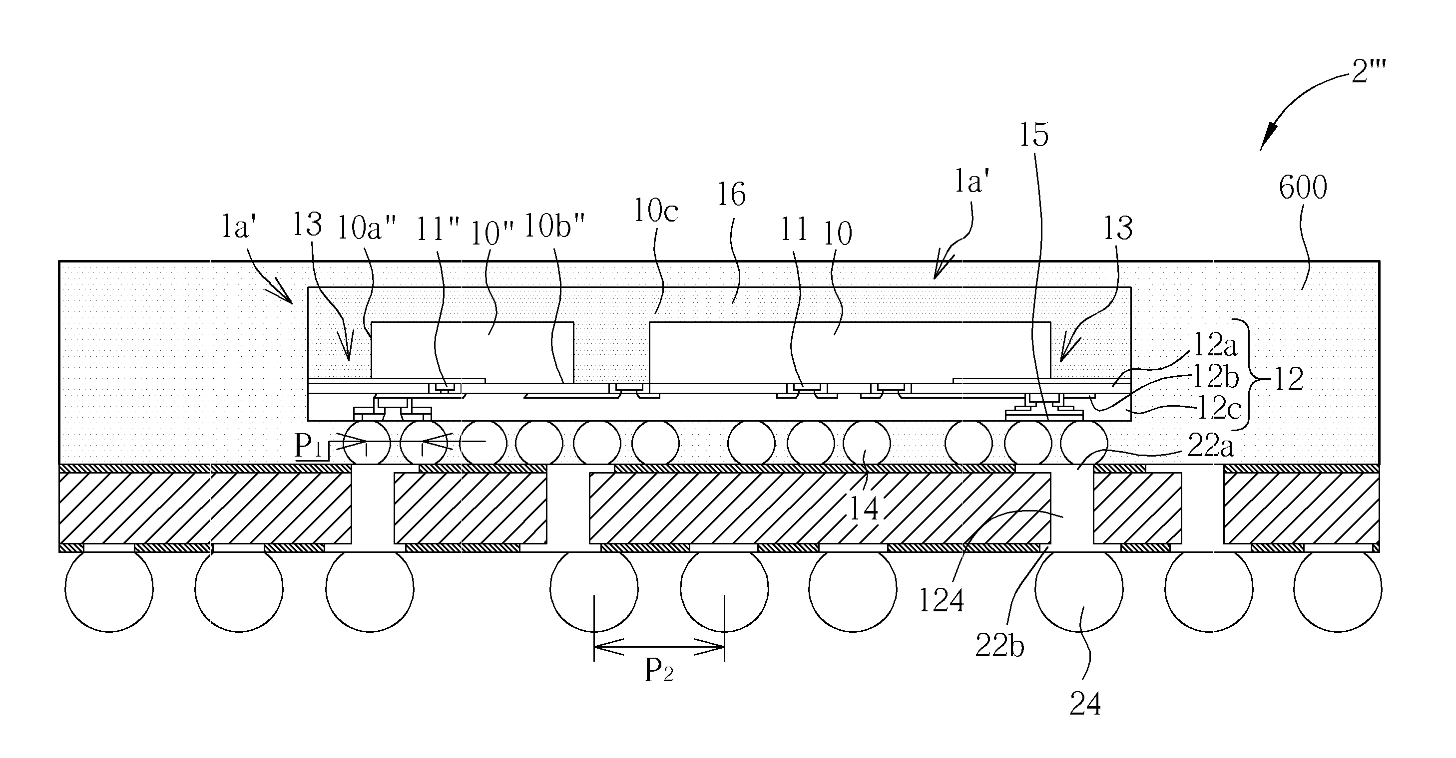
[0039]The present invention pertains to a flip-chip package for high-pin-count applications, which may involve the use of wafer-level packaging (WLP) technique. Wafer-level packaging (WLP) refers to the technique of packaging an integrated circuit at wafer level, instead of the traditional process of assembling the package of each individual unit after wafer dicing. WLP is essentially a true chip-scale packaging (CSP) technique, since the resulting package is practically of the same size as the die. Furthermore, wafer-level packaging paves the way for true integration of wafer fabrication, packaging, test, and burn-in at wafer level, for the ultimate streamlining of the manufacturing process undergone by a device from silicon start to customer shipment.

[0040]The present invention takes advantage of the WLCSP technology and fans out small pitch I / O pins or bumps on a chip such that the fan-out bond pads meet the minimum bump pitch requirement (e.g., 150 nm) of current flip-chip proce...


PUM


Abstract

A system-in-package includes a package carrier; a first semiconductor die having a die face and a die edge, the first semiconductor die being assembled face-down to a chip side of the package carrier; a second semiconductor die mounted alongside of the first semiconductor die; a rewiring laminate structure comprising a re-routed metal layer between the first semiconductor die and the package carrier. At least a portion of the re-routed metal layer projects beyond the die edge. A plurality of bumps are arranged on the rewiring laminate structure for electrically connecting the first semiconductor die with the package carrier.

Description

CROSS REFERENCE TO RELATED APPLICATIONS[0001]This is a continuation-in-part of U.S. application Ser. No. 12 / 370,537 filed Feb. 12, 2009, which claims the benefits from U.S. provisional application No. 61 / 056,401 filed May 27, 2008 and is hereby incorporated by reference. This application also claims the benefits from U.S. provisional application No. 61 / 347,494 filed May 24, 2010, which is hereby incorporated by reference.BACKGROUND OF THE INVENTION[0002]1. Field of the Invention[0003]The present invention relates generally to semiconductor packaging and, more particularly, to a flip-chip package for high-pin-count applications.[0004]2. Description of the Prior Art[0005]As known in the art, there are a variety of chip package techniques such as ball grid array (BGA), wire bonding, flip-chip, etc. for mounting a die on a substrate via the bonding points on both the die and the substrate. In order to ensure miniaturization and multi-functionality of electronic products or communication...

Claims


Application Information

Patent Timeline
Patent Type & Authority Patents(United States)
IPC IPC(8): H01L23/48
CPCH01L21/563H01L23/3128H01L23/3135H01L23/49816H01L23/49827H01L23/49833H01L23/5382H01L24/19H01L23/367H01L23/3672H01L23/3675H01L23/42H01L2224/16225H01L2224/73203H01L2224/73204H01L2924/01015H01L2924/01075H01L2924/01078H01L2924/01322H01L2924/14H01L2924/30107H01L2924/3011H01L2224/32225H01L2924/15311H01L2924/00H01L2924/01029H01L2224/12105H01L2224/73267H01L2924/181H01L2924/18162
Inventor CHEN, NAN-CHENGHSU, CHIH-TAI
Owner MEDIATEK INC
Why Eureka
Try Eureka