

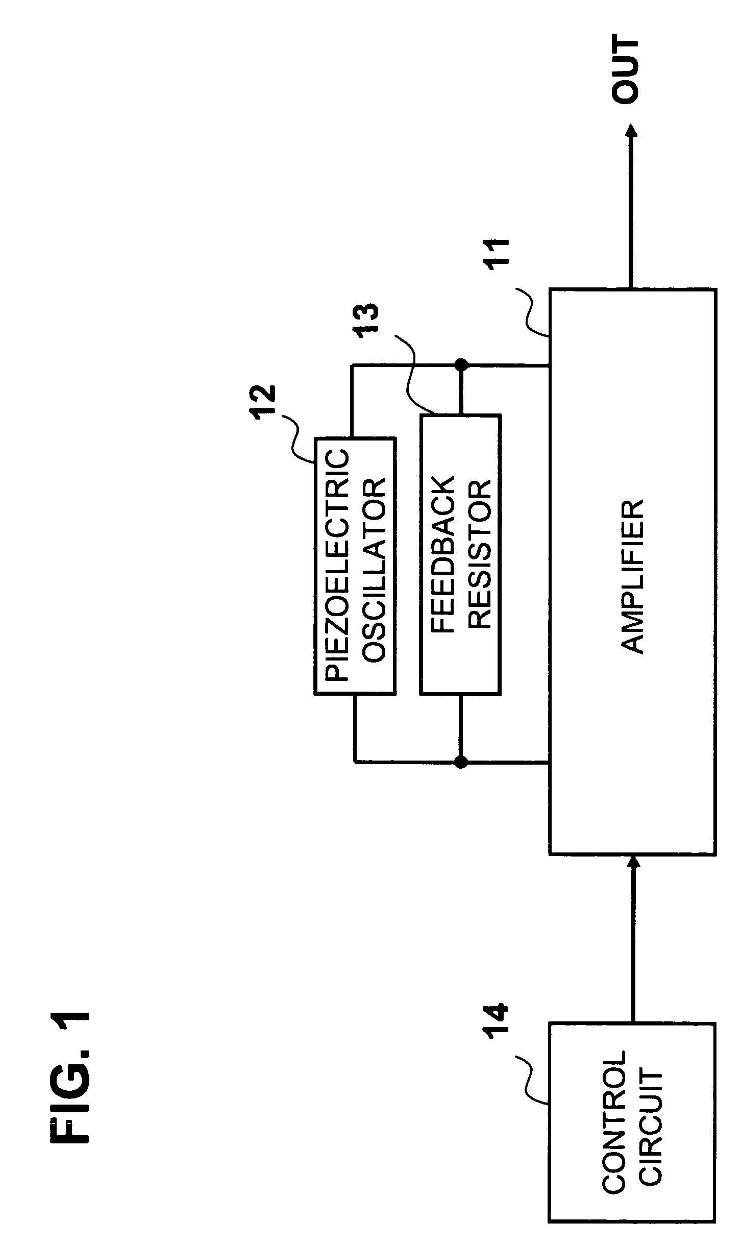
Oscillation circuit and method of controlling same
a technology of oscillation circuit and code signal, which is applied in the direction of oscillation generator, pulse technique, instruments, etc., can solve the problems of not being able to suppress the current consumption related to the start-up of the oscillation circuit, the time needed to transmit the code signal is very short, and the waste of current consumption cannot be suppressed. , to achieve the effect of suppressing wasteful current consumption, simple code relating to the key, and short time needed to transmit the code signal
- Summary
- Abstract
- Description
- Claims
- Application Information
AI Technical Summary
Benefits of technology
Problems solved by technology
Method used
Image

Examples
first exemplary embodiment
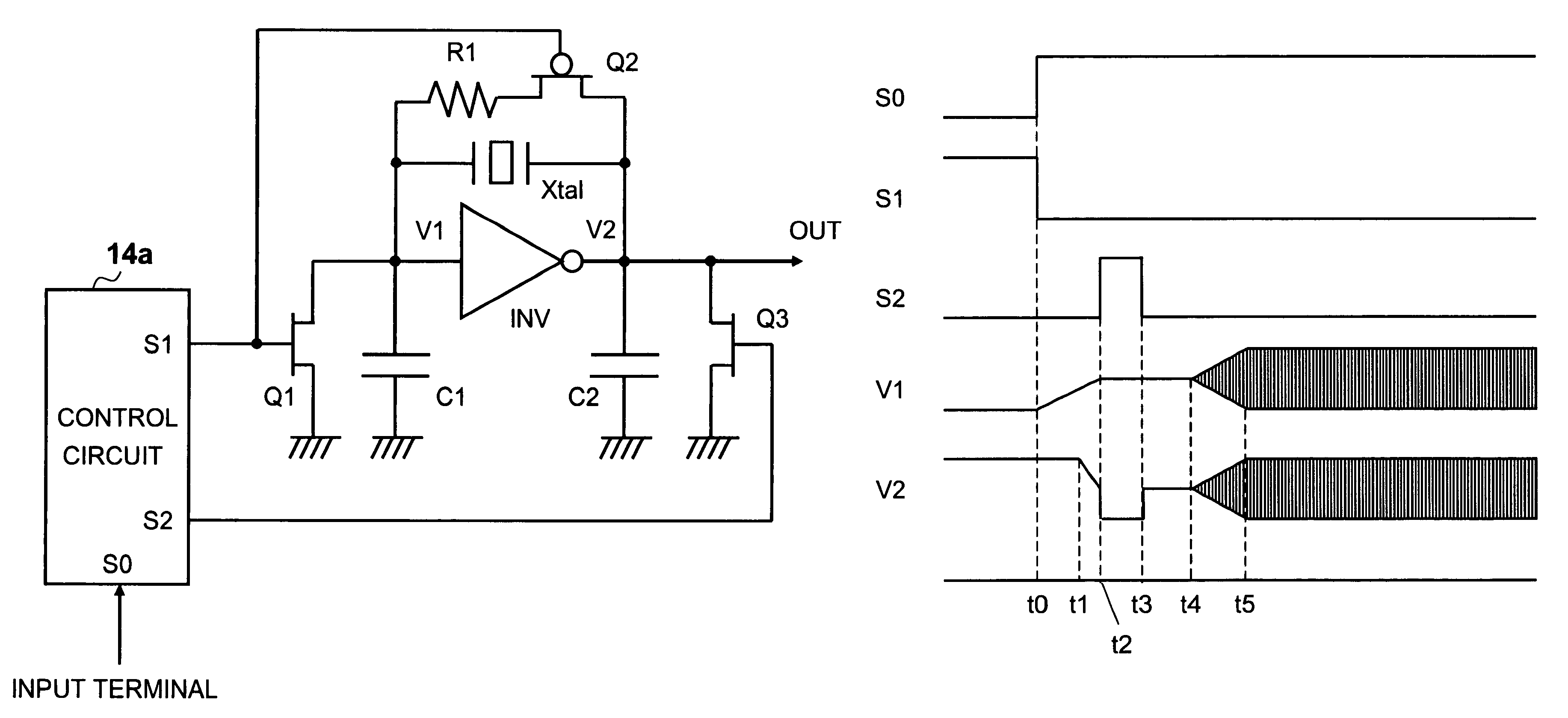
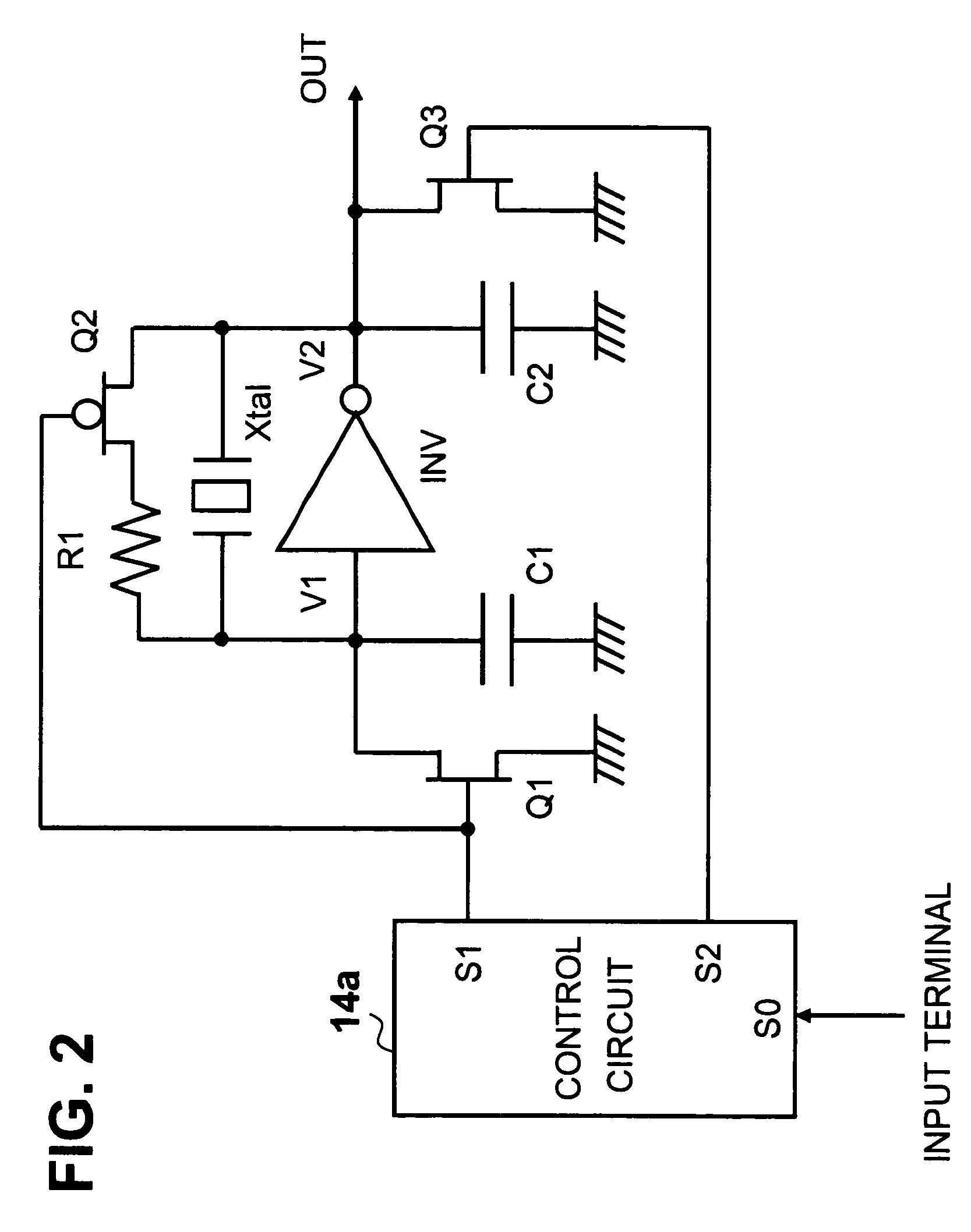
[0040]FIG. 2 is a circuit diagram of an oscillation circuit according to a first exemplary embodiment of the present invention. As shown in FIG. 2, the oscillation circuit includes a CMOS-configured inverter circuit INV, a crystal oscillator Xtal, a resistor R1, capacitors C1, C2, NMOS transistors Q1 Q3, a PMOS transistor Q2 and a CMOS-configured control circuit 14a.
[0041]The inverter circuit INV functions as an amplifier and has an input terminal to which are connected a first end of the capacitor C1, the drain of the NMOS transistor Q1, a first end of the crystal oscillator Xtal and a first end of the resistor R1, and an output terminal to which are connected a first end of the capacitor C2, the drain of the NMOS transistor Q3, a second end of the crystal oscillator Xtal and a first end of the PMOS transistor Q2. The second end of the PMOS transistor Q2 and the second end of the resistor R1 are connected to each other. The second end of the capacitor C1, the source of the NMOS tr...
second exemplary embodiment
[0051]FIG. 4 is a circuit diagram of an oscillation circuit according to a second exemplary embodiment of the present invention. Components in FIG. 4 identical with those in FIG. 2 are designated by like reference characters and need not be described again. The oscillation circuit according to the second exemplary embodiment differs from the oscillation circuit of FIG. 2 in that the NMOS transistor Q1 and PMOS transistor Q2 are eliminated and a 2-input NAND gate NAND is provided in place of the inverter circuit INV. Further, the control circuit 14b has a terminal SIB. A signal that is opposite in phase to the signal that is output from the terminal S1 of FIG. 2 is output from the terminal SIB to the first input terminal of the NAND gate NAND. The first end of the resistor R1, the first end of the capacitor C1 and the first end of the crystal oscillator Xtal are connected to the second input terminal of the NAND gate NAND. Further, the first end of the capacitor C2, the second end of...
third exemplary embodiment
[0059]FIG. 6 is a circuit diagram of an oscillation circuit according to a third exemplary embodiment of the present invention. Components in FIG. 6 identical with those in FIG. 2 are designated by like reference characters and need not be described again. The oscillation circuit according to the third exemplary embodiment differs from the oscillation circuit of FIG. 2 in that the NMOS transistor Q1 and PMOS transistor Q2 are eliminated and a 2-input NOR gate NOR is provided in place of the inverter circuit INV. The terminal S1 is connected to the first input terminal of the NOR gate NOR. The first end of the resistor R1, the first end of the capacitor C1 and the first end of the crystal oscillator Xtal are connected to the second input terminal of the NOR gate NOR. Further, the first end of the capacitor C2, the second end of the crystal oscillator Xtal, the second end of the resistor R1 and the drain of the NMOS transistor Q3 are connected to the output terminal of the NOR gate NO...
PUM
 Abstract
Description
Claims
Application Information