

Active inductor for ASIC application
a technology of active inductors and asics, applied in the field of modular active inductors, can solve the problems of large real estate requirements of conventional on-chip inductors fabricated using metal wiring layers, such as passive spiral inductors, and consume high power. , the quality factor q is relatively low
- Summary
- Abstract
- Description
- Claims
- Application Information
AI Technical Summary
Benefits of technology
Problems solved by technology
Method used
Image

Examples
Embodiment Construction
[0009]Accordingly, it is an object of the invention to provide a compact modular active inductor (MAI) which can be constructed using existing low cost, well-developed CMOS process integration techniques applicable to eDRAM and SRAM devices.
[0010]It is another object of the invention to optimize the utilization of the modular active inductor, wherein MAIs are arranged in an array configuration, with serial, parallel or combinations thereof to obtain a wide range of inductances.
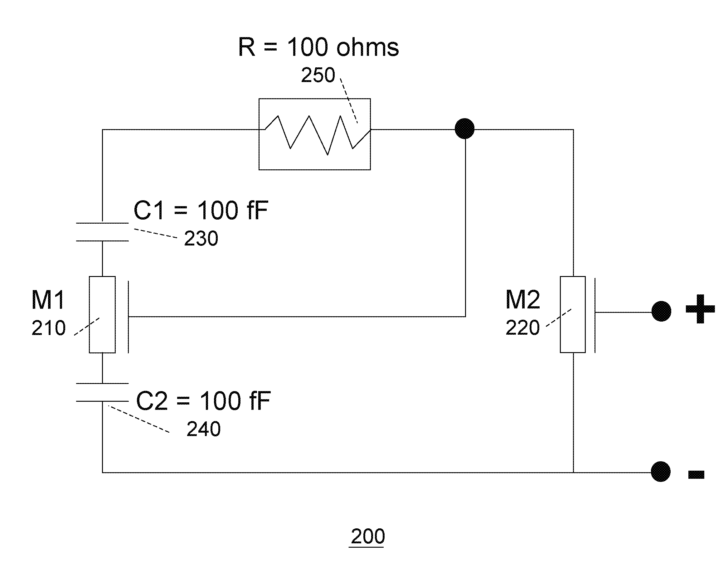
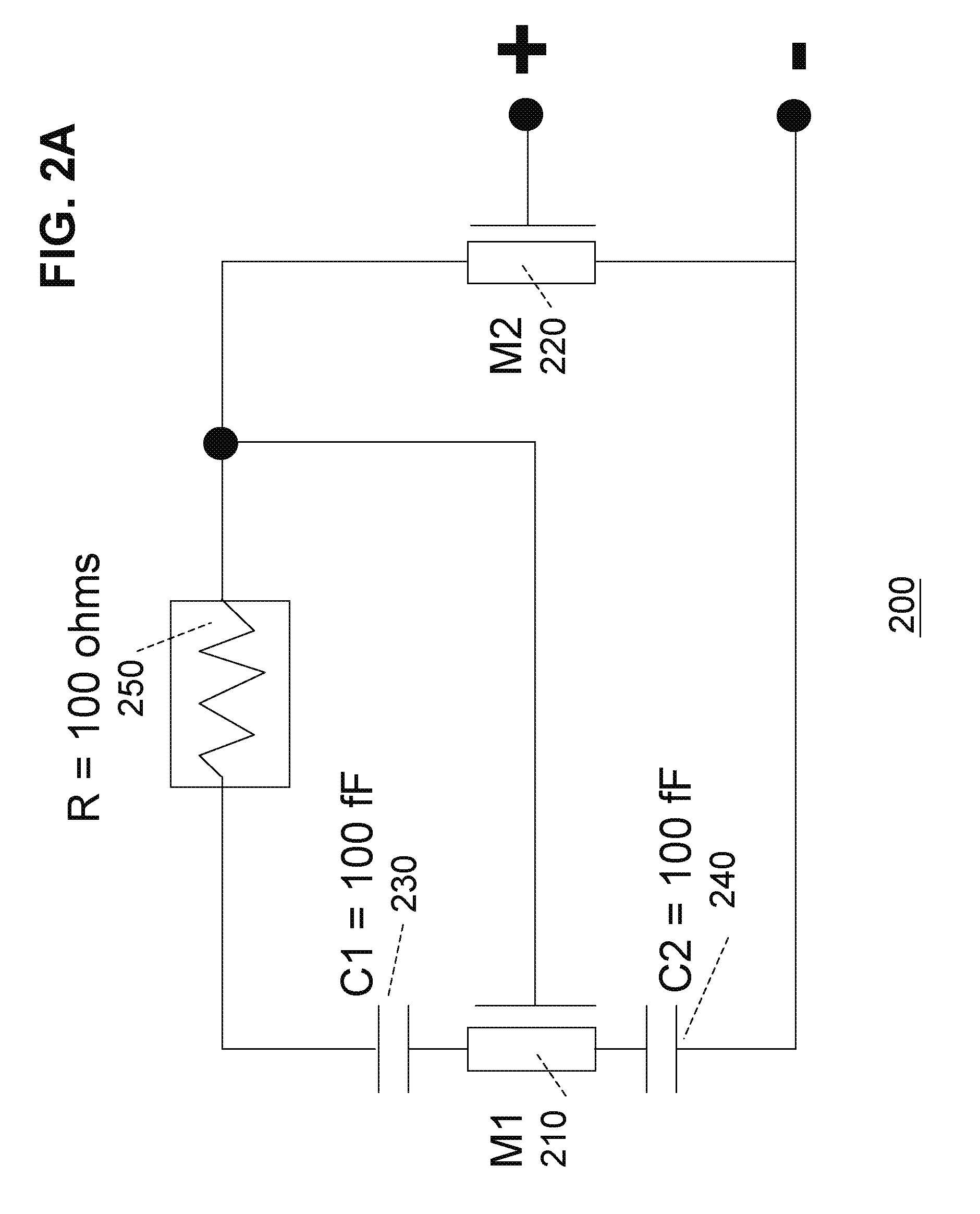
[0011]It is still another object to provide an active inductor module consisting of a minimum number of MOSFET devices, capacitors and resistor, and characterized by having a high quality factor Q and low parasitic resistance.
[0012]It is a further object to provide an MAI that is easily tunable and which can be adapted to a large variety of design applications.
[0013]These and other objectives are achieved in one embodiment of the present invention by an active inductor module with a circuit formed by only two ...
PUM
 Abstract
Description
Claims
Application Information