ROM cell having an isolation transistor formed between first and second pass transistors and connected between a differential bitline pair

a technology of isolation transistor and transistor, applied in the field of semiconductor memories, can solve problems such as lithography printing, line-end shortening, contact landing and cd uniformity, and difficulty in lithography printing,

Active Publication Date: 2012-02-21
TAIWAN SEMICON MFG CO LTD
View PDF5 Cites 25 Cited by
  • Summary
  • Abstract
  • Description
  • Claims
  • Application Information

AI Technical Summary

Benefits of technology

[0031]The ROM memory cell array and layout described herein utilizes fully symmetrical OD and gate layouts that provide improved lithography patterning process margins and device matching for improved electrical performance. With respect to electrical performance, the design layout provides a fully balanced STI stress effect on all cells even if those cells exhibit poly-to-OD misalignment. The layout improves the OD layer process margin and thus avoids the problems associated with small OD islands in prior art arrays. The same gate spacing is provided for each cell, thus providing fully balanced electrically performance across the array. The device, therefore, does not suffer from the so-called gate spacing effect.

Problems solved by technology

However, the single transistor cell structure provides shrinkage challenges for future technology generations, like OD minimum area (small island) induced lithography process margin and integration problems.
This layout results in problems relating to lithography printing, pattern lifting, line-end shortening, contact landing and CD uniformity.
The conventional layout also has issues with the landing margin when the contact is positioned at a line-end.
Differences in source / drain (S / D) area opening, as determined by the gate space, will result in a different junction distribution across the memory array, and therefore impact performance characteristics like device drive current, threshold voltage, and junction leakage.
This results in poor matching performance on cell devices and wide spreads in chip speed.
This effect also impacts yield.
Increasing transistor size (cell size) or decreasing the memory's operation speed can compensate for these layout environmental effects, but these modifications impact product cost and / or performance.

Method used


Image

  • ROM cell having an isolation transistor formed between first and second pass transistors and connected between a differential bitline pair
  • ROM cell having an isolation transistor formed between first and second pass transistors and connected between a differential bitline pair
  • ROM cell having an isolation transistor formed between first and second pass transistors and connected between a differential bitline pair

Examples


Embodiment Construction

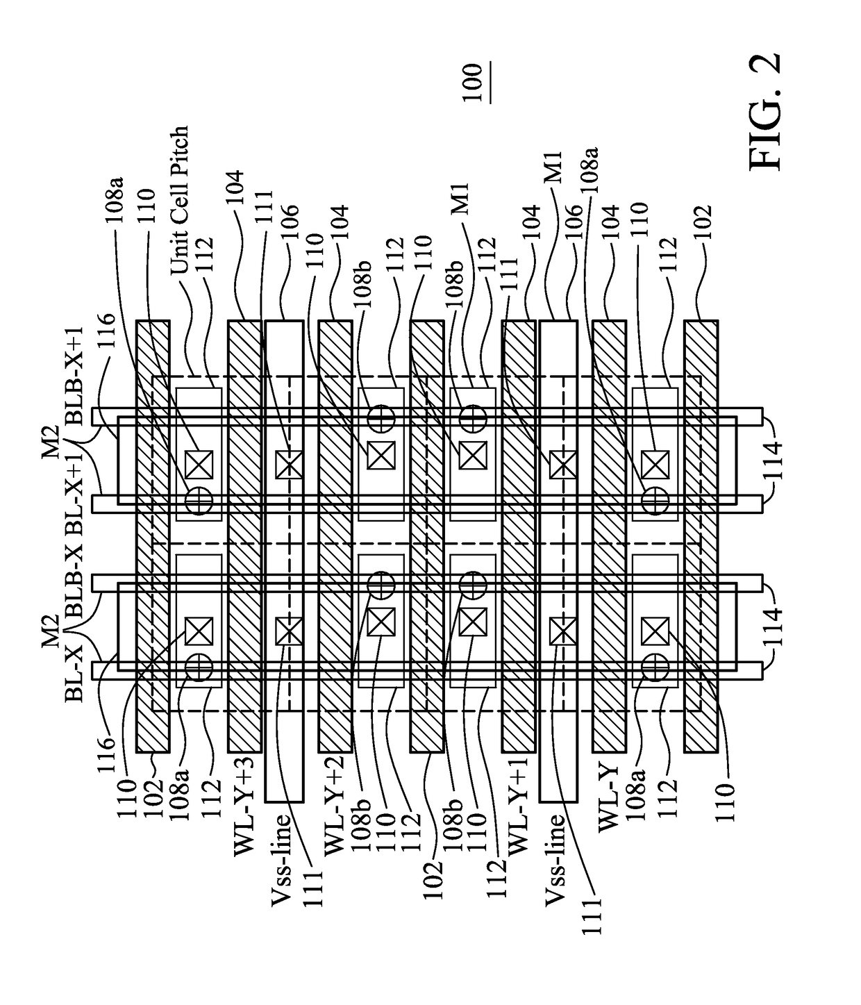
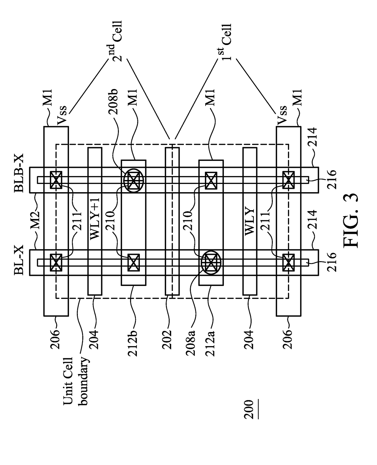
[0016]This description of the exemplary embodiments is intended to be read in connection with the accompanying drawings, which are to be considered part of the entire written description. In the description, relative terms such as “lower,”“upper,”“horizontal,”“vertical,”“above,”“below,”“up,”“down,”“top” and “bottom” as well as derivative thereof (e.g., “horizontally,”“downwardly,”“upwardly,” etc.) should be construed to refer to the orientation as then described or as shown in the drawing under discussion. These relative terms are for convenience of description and do not require that the apparatus be constructed or operated in a particular orientation. Terms concerning electrical communications and the like, such as, “coupled” and “electrically coupled” or “electrically connected,” refer to a relationship wherein nodes communicate with one another either directly or indirectly through intervening structures, unless described otherwise.

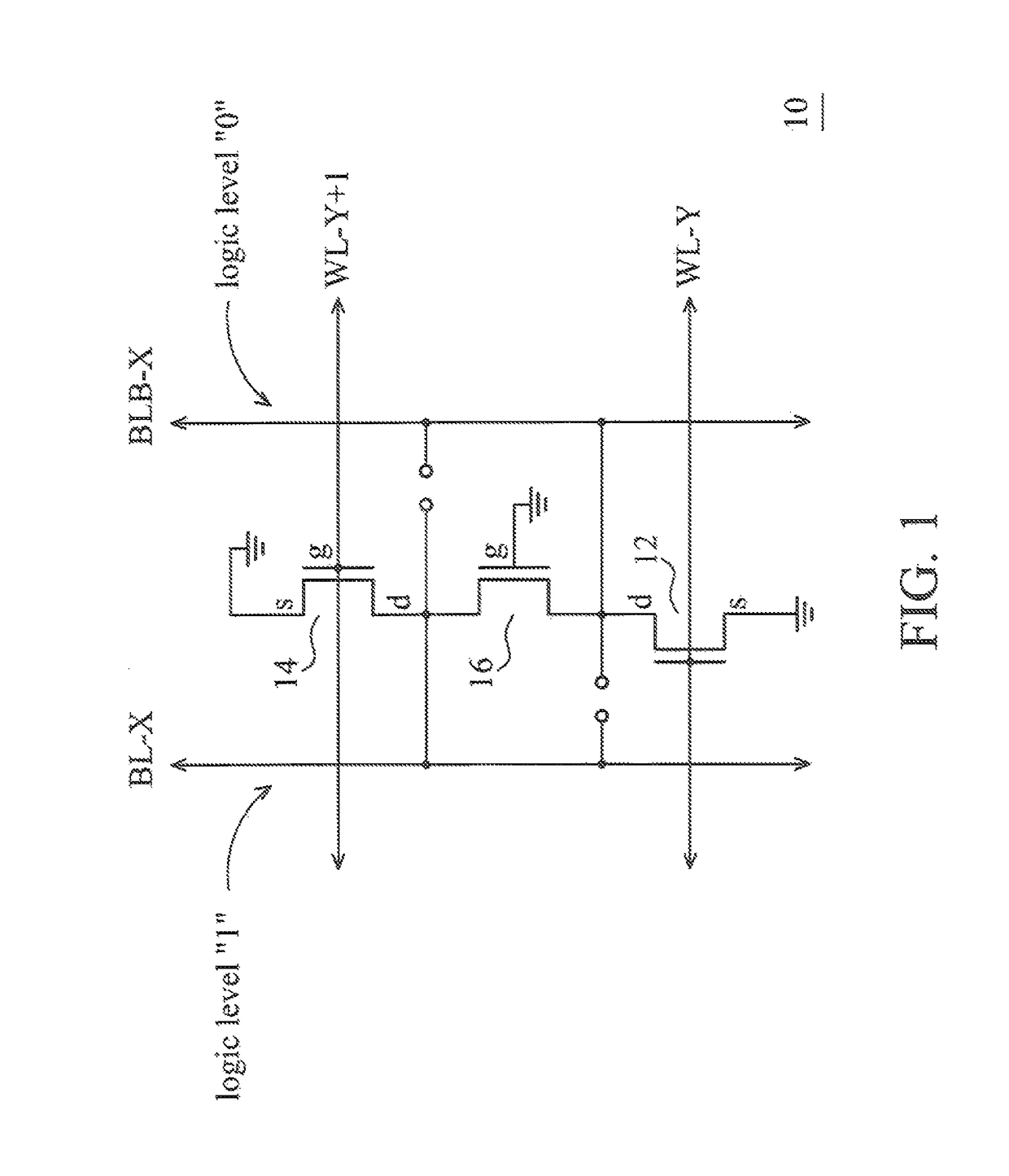
[0017]FIG. 1 is a circuit diagram of a portion ...


PUM


Abstract

A semiconductor memory cell array includes an elongated continuous active region. First and second pass transistors are formed in the elongated continuous active region and form part of first and second adjacent memory cells, respectively, of a column of memory cells in the array. An isolation transistor is formed in the elongated continuous active region between the first and second pass transistors and biased in an off state. First and second word lines are coupled to the gates of the pass transistors for applying a reading voltage. The array includes a differential bit line pair including first and second bit lines, a first logic value being encoded into the memory cells by connecting the pass transistors to the first bit line and a second logic value being encoded into the memory cells by connecting the pass transistors to the second bit line.

Description

CROSS-REFERENCE TO RELATED APPLICATIONS[0001]This application claims priority to U.S. provisional patent application No. 61 / 245,469 filed Sep. 24, 2009, entitled “ROM Cell and Array Structure”, the entirety of which is hereby incorporated by reference herein.FIELD OF THE INVENTION[0002]The present invention relates generally to semiconductor memories, and more particularly to semiconductor read-only-memory (ROM) cell array structures.BACKGROUND OF THE INVENTION[0003]Semiconductor ROM is a type of solid state memory that is fabricated with desired data permanently stored in it. The “on” or “off” state of each memory cell is set by programming the memory. Each memory cell is capable of storing a binary bit of data, representing either a logic state of “0” or “1” depending on whether the path of a bit line to ground (VSS) of the memory cell is electrically connected or electrically isolated.[0004]Designers prefer simple schemes like single end circuits (e.g., inverters) to detect the d...

Claims


Application Information

Patent Timeline
Patent Type & Authority Patents(United States)
IPC IPC(8): G11C17/10
CPCG11C17/12H01L27/0207
Inventor LIAW, JHON JHY
Owner TAIWAN SEMICON MFG CO LTD
Why Eureka
Try Eureka