Electron-emitting device, method of manufacturing the same, electron source, and image display apparatus

a technology of electron-emitting device and manufacturing method, which is applied in the manufacture of electrode systems, electric discharge tubes/lamps, and discharge systems, etc., can solve the problems of discharge break-down, reduced electron-emitting efficiency, and insufficient gap between the extending portions, etc., to achieve excellent electron-emitting efficiency, stable electron-emitting characteristics, and large electron-emitting amoun

Inactive Publication Date: 2012-02-28
CANON KK
View PDF5 Cites 0 Cited by
  • Summary
  • Abstract
  • Description
  • Claims
  • Application Information

AI Technical Summary

Benefits of technology

[0009]The present invention has been made in view of the problems described above. An object of the present invention is to provide an electron-emitting device which is excellent in electron-emitting efficiency and capable of obtaining a large electron-emitting amount and stable electron-emitting characteristics. Another object of the present invention is to provide an electron source which uses the electron-emitting device and thus which is excellent in uniformity and stability and obtains a large electron-emitting amount, and an image display apparatus which uses the electron-emitting device and thus which is excellent in display characteristics.
[0015]According to the electron-emitting device of the present invention, the carbon films have the excellent gaps even in the extending portions, and hence problems such as the generation of leak current and the discharge break-down of the electron-emitting device which are due to the defective formation of the gaps are prevented. Therefore, the electron-emitting device can stably emit electrons from the gap between the conductive films and the gaps between the carbon films. Thus, a larger electron-emitting amount and more excellent electron-emitting efficiency can be obtained as compared with a conventional electron-emitting device.
[0016]The image display apparatus using the electron-emitting device according to the present invention realizes lower power consumption and high luminance and can stably display a high-quality image.

Problems solved by technology

However, a sufficient gap cannot be provided between the extending portions of the pair of carbon films depending on formation conditions, and hence there is a case where end sections (sections apart from the conductive films) of the extending portions are connected to each other.
When the extending portions of the carbon films are connected to each other as described above, an ineffective current (leak current) flows between the device electrodes through the extending portions, and, as a result, there is a case where electron-emitting efficiency reduces.
Long time driving or vacuum atmosphere reduction tends to cause discharge break-down.

Method used


Image

  • Electron-emitting device, method of manufacturing the same, electron source, and image display apparatus
  • Electron-emitting device, method of manufacturing the same, electron source, and image display apparatus
  • Electron-emitting device, method of manufacturing the same, electron source, and image display apparatus

Examples


example 1

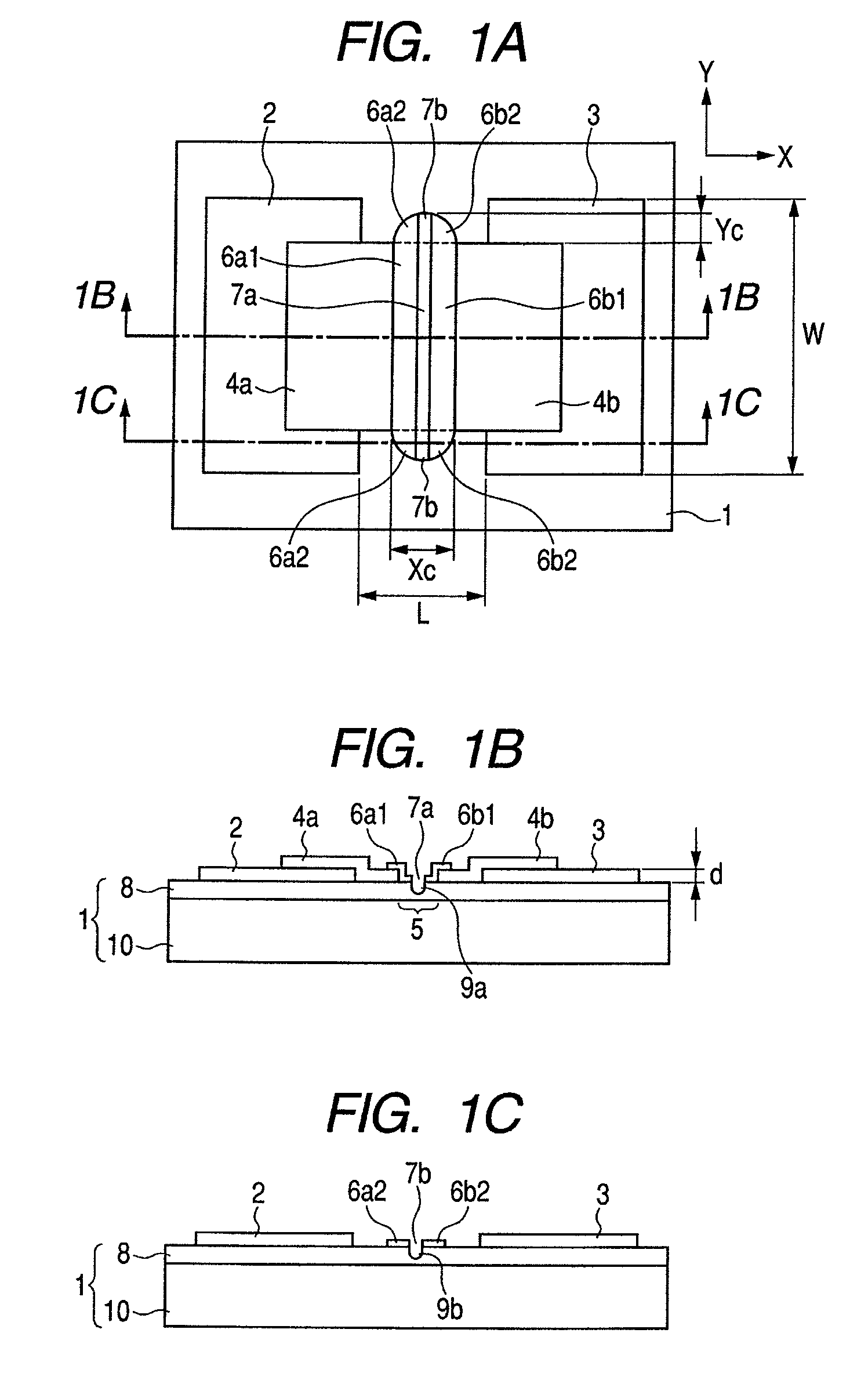
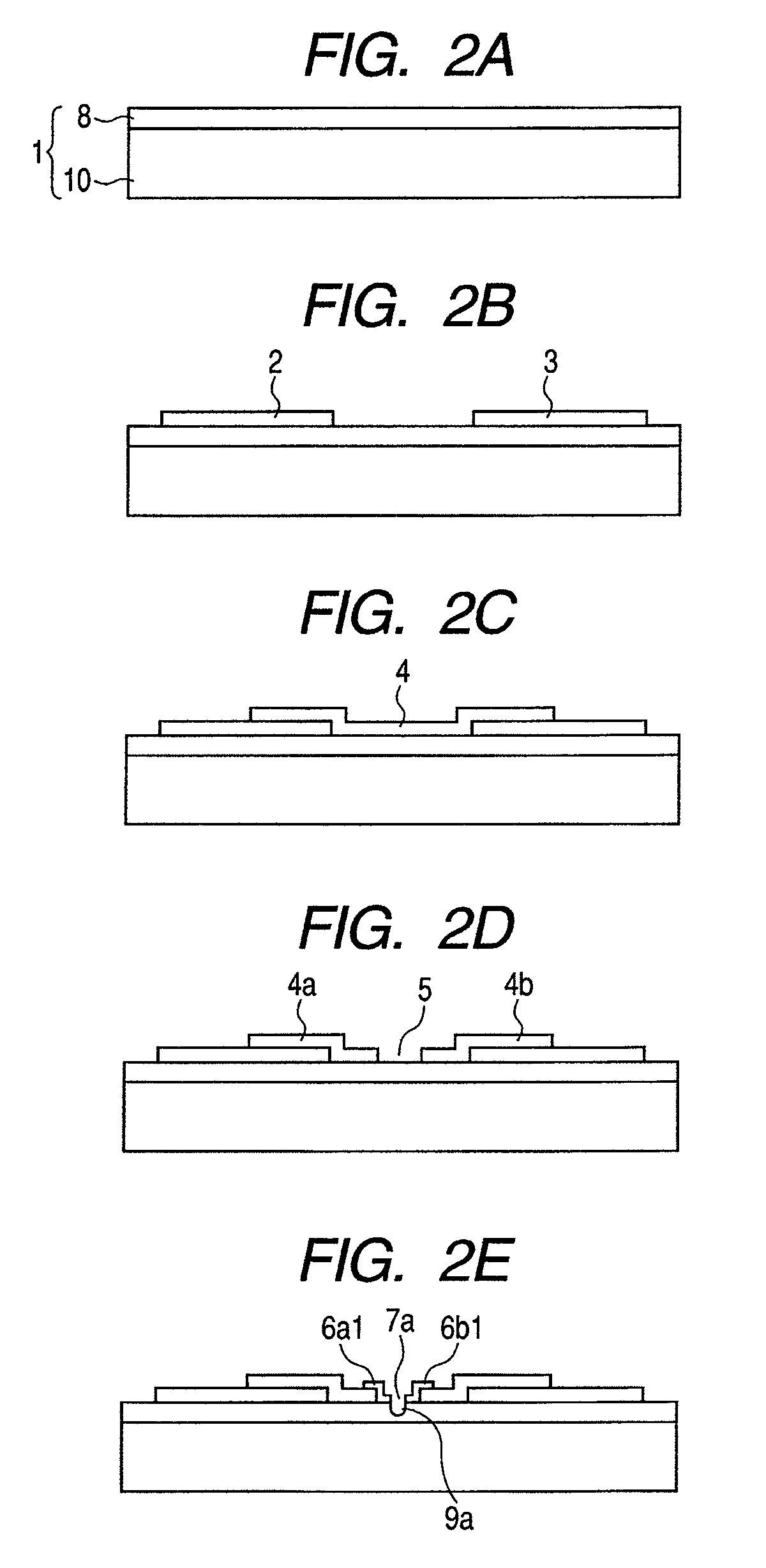
[0100]The electron-emitting device illustrated in FIGS. 1A to 1C was manufactured through the steps illustrated in FIGS. 2A to 2E.

[0101](Step-a)

[0102]The glass base material 10 (produced by Asahi Glass Co. Ltd., PD200) was sufficiently cleaned with a cleaning solution, deionized water, and an organic solvent. Then, the passivation layer 8 made of SiO2 was deposited on the base material 10 at a thickness of approximately 250 nm using an Rf sputtering apparatus, to prepare the substrate 1 (FIG. 2A).

[0103](Step-b)

[0104]A Ti layer having a thickness of 5 nm and a Pt layer having a thickness of 40 nm were successively deposited on the substrate 1 by a sputtering process. Then, an etching mask (photoresist) was formed so as to cover a pattern of the first and second electrodes 2 and 3. Next, dry etching using Ar plasma was performed and subsequently a remaining portion of the etching mask was removed by dissolving to form the first and second electrodes 2 and 3 (FIG. 2B). The interval L b...

example 2

[0128]An electron-emitting device manufactured in this example is different from Example 1 in that the passivation layer 8 is not used. Hereinafter, a method of manufacturing the electron-emitting device according to this example is described step by step with reference to FIGS. 2A to 2E.

[0129](Step-a)

[0130]A quartz glass substrate was sufficiently cleaned with deionized water and an organic solvent to prepare the substrate 1.

[0131]Step-b to Step-d were performed in the same manner as in Example 1.

[0132]Step-e and Step-f were performed in the same manner as in Example 1, except that the peak was adjusted to ±15 V.

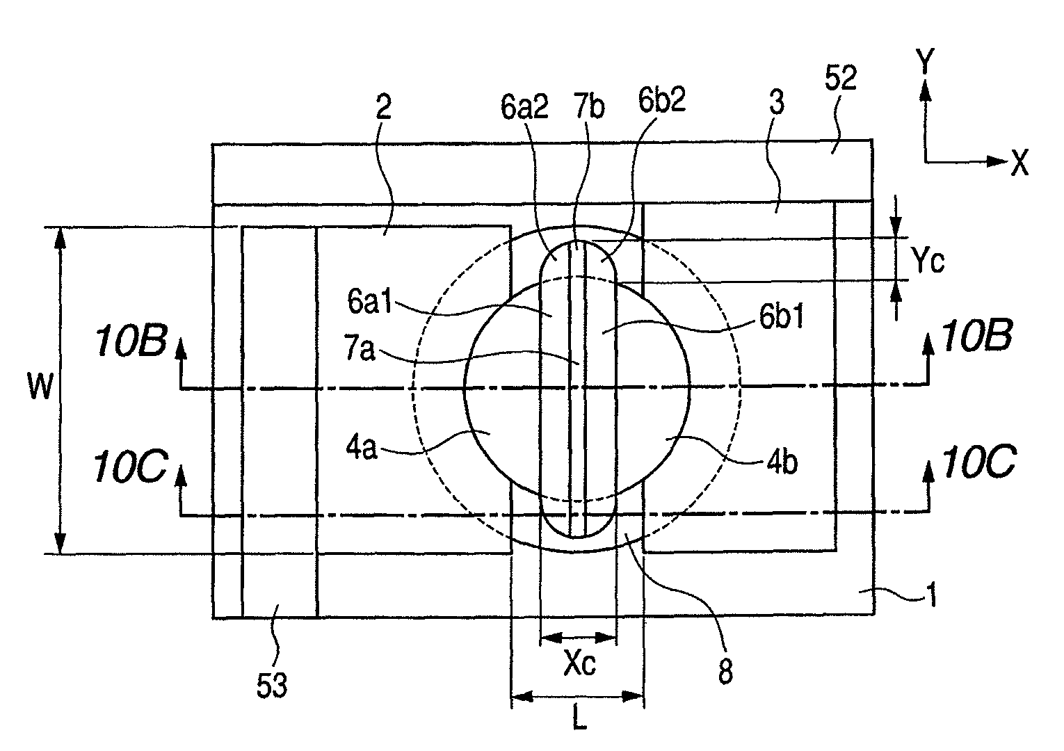
[0133]After the steps, an observation using an optical microscope was performed. As a result, it was determined that the electron-emitting device having the structure schematically illustrated in FIG. 1A was obtained. In the first and second extending portions 6a2 and 6b2, Xc of FIG. 1A was 9.2 μm and Yc of FIG. 1A was 3.2 μm.

[0134]The first and second extending portions 6a...

example 3

[0142]FIG. 9 is an explanatory view illustrating an electron-emitting device according to this example.

[0143]The electron-emitting device according to this example is different from that of Example 1 in that the conductive film 4 of the electron-emitting device according to Example 1 was formed by an ink-jet process and the passivation layer 8 was formed using a polysilazane solution. Others are fundamentally performed in the same manner as in Example 1.

[0144]Hereinafter, a method of manufacturing the electron-emitting device according to this example is described step by step with reference to FIG. 9 and FIGS. 2A to 2E.

[0145](Step-a)

[0146]A glass substrate made of soda lime glass was sufficiently cleaned with a cleaning solution, deionized water, and an organic solvent. The polysilazane solution, Aquamica (produced by AZ Electronic Materials, NN110-20) was spin-applied onto the glass substrate for 30 seconds at 2,000 revolutions / minute. Subsequently, the glass substrate was dried a...


PUM


Abstract

Provided is an electron-emitting device which is excellent in electron-emitting efficiency, and may obtain a large electron-emitting amount and stable electron-emitting characteristics. The electron-emitting device includes: a first conductive film and a second conductive film which are provided through a first gap; first carbon films connected to the first conductive film; and second carbon films which are connected to the second conductive film, and are opposed to the first carbon films through second and third gaps. Continuous concave portions are provided in the second and third gaps.

Description

BACKGROUND OF THE INVENTION[0001]1. Field of the Invention[0002]The present invention relates to an electron-emitting device used for a flat panel display, and a method of manufacturing the electron-emitting device, an electron source including the electron-emitting device, and an image display apparatus using the electron source.[0003]2. Description of the Related Art[0004]A surface conduction electron-emitting device is based on the phenomenon that a conductive film formed on an insulating substrate is supplied with a current in parallel to a surface of the conductive film, to emit electrons. Fundamentally, a pair of device electrodes are formed on the substrate. The conductive film is formed so as to connect the device electrodes to each other. A minute gap is provided in the conductive film to form a pair of conductive films. An operation called “activation” is performed to deposit a pair of carbon films in the gap and on portions of the conductive films which are close to the g...

Claims


Application Information

Patent Timeline
Patent Type & Authority Patents(United States)
IPC IPC(8): H01J63/04
CPCH01J1/316H01J9/027H01J31/127H01J2201/3165H01J2329/0489
Inventor SHIMAZU, AKIRA
Owner CANON KK
Why Eureka
Try Eureka