Electrostatic latent image measuring device

a technology measuring device, which is applied in the field of electrostatic latent image measuring device and electrostatic latent image measuring method, can solve the problems of inability to obtain real-time condition of electrostatic latent image, difficulty in measuring electrostatic latent image, etc., and achieve high accuracy

Active Publication Date: 2012-03-27
RICOH KK
View PDF46 Cites 6 Cited by
  • Summary
  • Abstract
  • Description
  • Claims
  • Application Information

AI Technical Summary

Benefits of technology

[0080]It is, therefore, an object of the present invention to provide an electrostatic latent image measuring device and an electrostatic latent image measuring method which can measure a size of an electrostatic latent image with high accuracy by measuring a coordinate of a sample relative to the change in an observation area by electrification without damaging the sample, and an image forming device having an image carrier measured by using the electrostatic latent image measuring device and the electrostatic latent image measuring method.
[0081]It is also an object of the present invention to provide an electrostatic latent image measuring device, an electrostatic latent image measuring method and an image forming device which irradiate a charged particle beam and form an electrostatic latent image on a photoconductor, and measures the photoconductor condition having the electrostatic latent image in a short time and with high resolution without causing damage.
[0096]Preferably, the exposure optical system includes a second adjuster which adjusts the scanning light in a predetermined range and can adjust the exposure optical system in an incident axis direction or a horizontal direction.

Problems solved by technology

However, it is extremely difficult to measure an electrostatic latent image, and an actual image forming device can not measure the electrostatic latent image at present.
However, a method of measuring an electrostatic latent image which visually displays the results of the measurement has not been obtained yet.
However, in these devices, it is necessary to move the head sensor closer to the sample.
In the measurement method performed many times, an actual electrostatic latent image can not be measured because natural discharge or absorption of a substance occurs during the measurement, and the condition of the latent image varies from hour to hour during the measurement by the influence of the sensor itself, so that the real-time condition of the electrostatic latent image can not be obtained.
However, in these methods, since the development and transfer processes are conducted, the electrostatic latent image is not directly measured.
However, considering a conductive property of a semiconductor such as Si, the material of the photoconductor is rather an insulating material, so that such a measuring method can not be applied to measure a photoconductor sample.
For this reason, this method can not be directly applied to a general photoconductor.
However, in the photoconductor, the electric charge can not be maintained for a long period of time because the photoconductor has some conductive property, so that the surface potential of the photoconductor is lowered by dark decay with time.
In this method, the resolution is low at about several millimeters, and 1 micron resolution can not be obtained.
However, this evaluation is conducted on a conductive portion in the LSI in which a current flows, the electric potential is low at about +5V, and also an electric potential is limited.
In the conventional observation method, a sample is limited to an LSI chip or a sample capable of storing and maintaining an electrostatic latent image.
However, since the resistance value of the photoconductor is not infinity, the electric charge can not be maintained for a long period of time in the photoconductor.
As a result, a desired electrostatic latent image can not be formed.
As another problem, there is a problem that the scanning area is changed if the sample is charged.
It is difficult to previously estimate the amount of change in the scanning area because various conditions such as a charging electric potential and a height of a sample are changed.
However, since the standard material is generally a conductive sample, the standard sample can not be charged.
An insulated sample can be charged, but a desired charging electric potential can not be applied to a desired area which becomes a standard, and the electric charge can not be removed in the insulated sample.
However, the photoconductor sample is easily affected by electrostatic fatigue and light fatigue, so that the charging condition is changed, and the photoconductor sample can not be used as the standard sample.

Method used


Image

  • Electrostatic latent image measuring device
  • Electrostatic latent image measuring device
  • Electrostatic latent image measuring device

Examples


embodiment 2

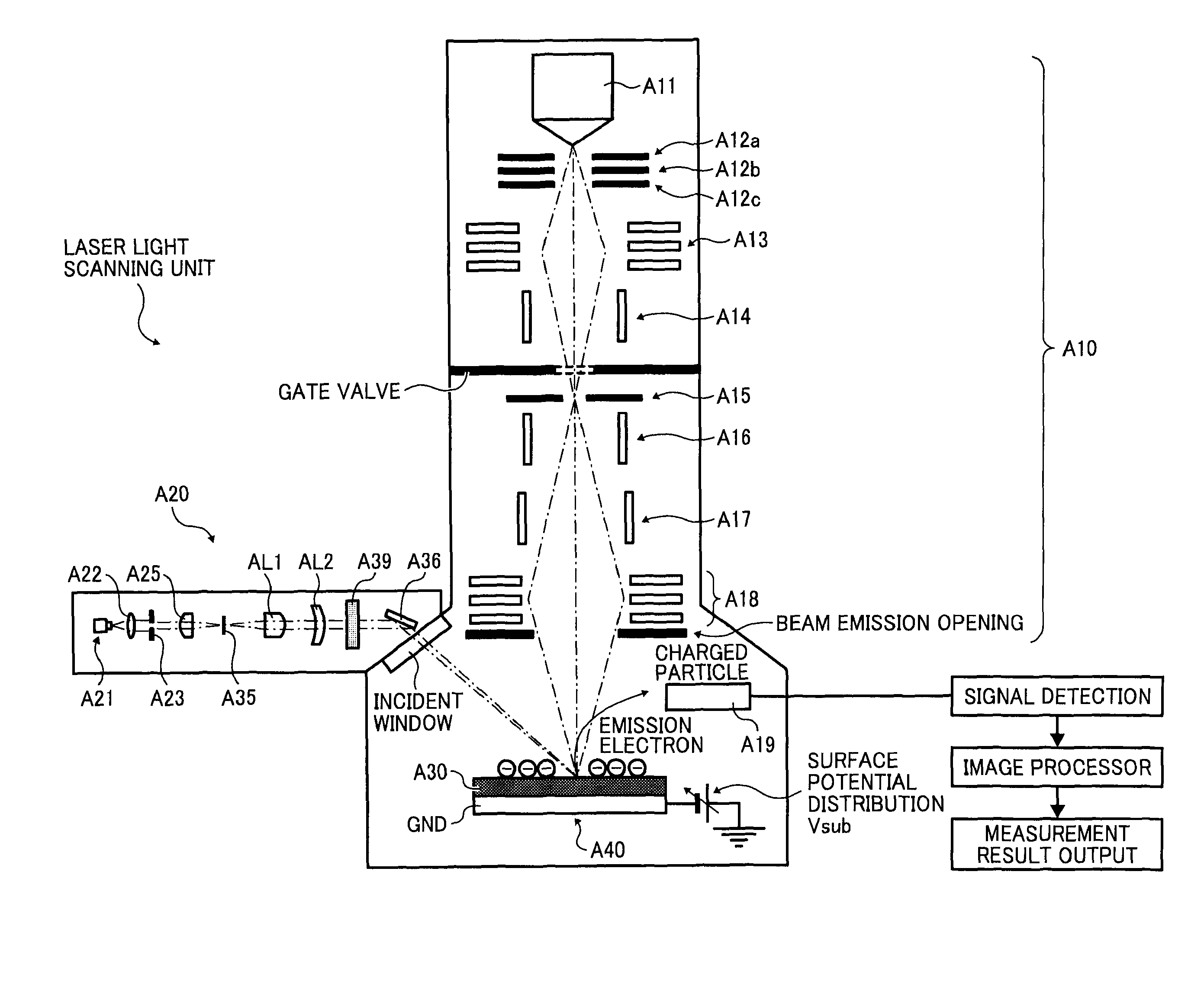
[0334]Next, an electrostatic latent image measuring device according to Embodiment 2 of the present invention will be described.

[0335]FIG. 16 illustrates the electrostatic latent image measuring device of this embodiment.

[0336]In this embodiment, most of the parts are the same as those in Embodiment 1, so the same reference numbers are applied to the same parts and the description will be omitted or simplified. Hereinafter, different parts from Embodiment 1 will be specifically described.

[0337]If the surface of the photoconductor sample includes an electric charge distribution, an electric field distribution according to the electric charge distribution on the surface is formed in a space.

[0338]For this reason, the secondary electron generated by the incident electron is brought back by this electric field, and the number of electrons which reach the detector is reduced.

[0339]A contrast image according to the electric charge distribution on the surface is thereby detected, in which ...

embodiment 3

[0443]In this embodiment, an electrostatic latent image is formed on the photoconductor by irradiating the charged particle beam, and the condition of the photoconductor onto which the electrostatic latent image is formed is measured with high resolution in a short time without destroying the latent image.

[0444]Moreover, a device which can quantitatively evaluates a beam profile of an electrostatic latent image with high accuracy and can be actually used for not only the beam profile but also an electrophotographic device, or evaluate an electrostatic latent image obtained by a photoconductor by dynamically conducting beam scanning, a device which can measure the influence on the formation of the latent image such as a reciprocity failure by multi-exposure or can generate and reproduce these phenomenon on the photoconductor, and a device which can measure and evaluate an electrostatic latent image on the photoconductor, a residual image and time degradation, can be achieved.

[0445]In...


PUM

PropertyMeasurementUnit
sizeaaaaaaaaaa
distanceaaaaaaaaaa
electric potentialaaaaaaaaaa

Abstract

An electrostatic latent image measuring device includes a charged particle optical system which irradiates an electron beam and charges a photoconductor sample, an exposure optical system which forms an electrostatic latent image on a surface of the photoconductor sample, and a scanning unit which scans the surface of the photoconductor sample by the electron beam, a distribution of the electrostatic latent image on the surface of the sample being measured by a signal detected by the scanning.

Description

PRIORITY CLAIM[0001]The present application is based on and claims priorities from Japanese Patent Applications No. 2008-048761, filed on, Feb. 28, 2008, and No. 2008-064114, filed on Mar. 13, 2008, the disclosures of which are hereby incorporated by reference in their entirety.BACKGROUND OF THE INVENTION[0002]1. Field of the Invention[0003]The present invention relates to an electrostatic latent image measuring device, an electrostatic latent image measuring method, and an image forming device, which measure a surface potential distribution and a surface charge distribution of a photoconductor and analyze the surface.[0004]2. Description of the Related Art[0005]An electrophotographic image forming device such as a copying machine or a printer uses a photoconductor.[0006]The following processes are performed relative to the photoconductor.[0007]A charging process which uniformly charges the electrophotographic photoconductor.[0008]An exposing process irradiates light corresponding t...

Claims


Application Information

Patent Timeline
Patent Type & Authority Patents(United States)
IPC IPC(8): G03G15/00G01N27/60
CPCG03G15/5037
Inventor SUHARA, HIROYUKIKUBO, NOBUAKI
Owner RICOH KK
Why Eureka
Try Eureka