Carbon nanotube high frequency transistor technology

a carbon nanotube and transistor technology, applied in the field of carbon nanotube transistor technology, can solve the problems of pushing the boundaries of silicon material, increasing performance requirements, etc., and achieve the effect of improving performance and efficiency of carbon nanotube transistor devices, and significantly reducing the distance between the ga

Inactive Publication Date: 2012-05-01
ETAMOTA CORP
View PDF42 Cites 32 Cited by
  • Summary
  • Abstract
  • Description
  • Claims
  • Application Information

AI Technical Summary

Benefits of technology

[0011]The present invention relates to transistor devices and associated methods making such devices using carbon nanotube technology. In an embodiment, the transistors include carbon nanotubes and more specifically, single-walled carbon nanotubes (SWNT). A technique of the invention reduces significantly the distance between the gate and single-walled carbon nanotubes to improve performance and efficiency of a carbon nanotube transistor device. Without using a porous template structure, single-walled carbon nanotubes are grown perpendicularly to a substrate between a base metal layer and a middle mesh layer. The nanotubes are insulated with a thin insulator and then gate regions are formed.

Problems solved by technology

However, demand for increasing performance requirements is pushing the boundaries of silicon material.

Method used


Image

  • Carbon nanotube high frequency transistor technology
  • Carbon nanotube high frequency transistor technology
  • Carbon nanotube high frequency transistor technology

Examples


Embodiment Construction

[0031]The invention provides a carbon nanotube device and techniques for manufacturing such a device, especially a transistor device. In a specific embodiment, the carbon nanotube device is a single-wall carbon nanotube (SWNT) transistor, where the single-walled carbon nanotube is an element of the transistor. A specific application of a single-wall carbon nanotube device of the invention is as a power transistor, a type of transistor capable of passing relatively high currents compared to standard transistors. Carbon nanotube transistors of the invention may be fabricated independently or in combination with devices and with devices of different technologies.

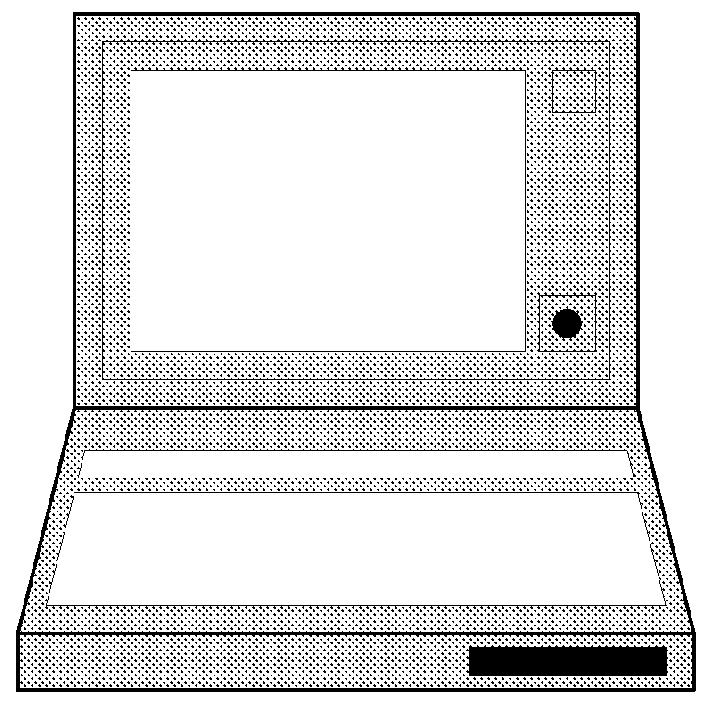
[0032]FIG. 1 shows an example of an electronic system incorporating one or more carbon nanotube transistors or rectifying devices of the invention, or combinations of these. Electronic systems come in many different configurations and sizes. Some electronic systems are portable or handheld. Such portable systems typically may b...


PUM

PropertyMeasurementUnit
output voltageaaaaaaaaaa
diametersaaaaaaaaaa

Abstract

A technique of the invention reduces significantly the distance between the gate and single-walled carbon nanotubes to improve performance and efficiency of a carbon nanotube transistor device. Without using a porous template structure, single-walled carbon nanotubes are grown perpendicularly to a substrate between a base metal layer and a middle mesh layer. The nanotubes are insulated with a thin insulator and then gate regions are formed.

Description

CROSS-REFERENCE TO RELATED APPLICATIONS[0001]This application claims the benefit of U.S. provisional patent application 60 / 882,890, filed Dec. 29, 2006, which is incorporated by reference along with all other references cited in this application. U.S. patent application Ser. No. 11 / 162,548, filed Sep. 14, 2005, is incorporated by reference.BACKGROUND OF THE INVENTION[0002]The present invention relates to semiconductor devices and their manufacture, and more specifically to carbon nanotube transistor technology.[0003]The age of information and electronic commerce has been made possible by the development of transistors and electronic circuits, and their miniaturization through integrated circuit technology. Integrated circuits are sometimes referred to as “chips.” Many numbers of transistors are used to build electronic circuits and integrated circuits. Modern microprocessor integrated circuits have over 50 million transistors and will have over 1 billion transistors in the future.[0...

Claims


Application Information

Patent Timeline
Patent Type & Authority Patents(United States)
IPC IPC(8): H01L29/72
CPCB82Y10/00B82Y30/00B82Y40/00C25D1/006C25D1/02C25D9/04H01L51/0003H01L51/057H01L29/0676H01L51/0006H01L51/0048Y10S977/742Y10S977/938Y10S977/767H10K71/125H10K71/12H10K85/221H10K10/491
Inventor LIM, BRIAN Y.LAI, JON W.
Owner ETAMOTA CORP
Why Eureka
Try Eureka