Infrared detecting device and manufacturing method thereof

a technology of infrared detection and manufacturing method, which is applied in the direction of optical radiation measurement, instruments, material analysis, etc., can solve the problems of large size and high cost, cumbersome maintenance, and the inability to make so thin beam portions, so as to reduce resistance and cost

Inactive Publication Date: 2012-05-15
LAPIS SEMICON CO LTD
View PDF8 Cites 0 Cited by
  • Summary
  • Abstract
  • Description
  • Claims
  • Application Information

AI Technical Summary

Benefits of technology

[0022]Therefore, the present invention has been invented in view of the above-described conventional technical problems. It is an object of the present invention to provide an infrared detecting device which suppresses the number of steps and makes the width of a beam portion narrower thereby to enable an improvement in device characteristics, and a manufacturing method thereof.
[0044]eliminating the semiconductor substrate by etching from an area in which the semiconductor substrate is exposed, thereby forming an air gap below the thermoelectric transducing part, the conductive material layer and the insulating material film located therearound.
[0045]In the method according to the present invention, parts of the insulating material film and the conductive material layer can be eliminated by etching in such a manner that the conductive material layer and each of the beam portions become identical in width, in the step for forming the beam portions.
[0048]According to the present invention, since a conductive material layer such as a metal silicide layer is also batch-processed upon beam-portion shape processing, an alignment error in a photolithography / etching process, which has presented a conventional problem, can be completely eliminated. It is therefore possible to bring the width of each beam portion to half or less of that employed in a conventional structure.
[0049]According to the present invention as well, since the conductive material layer such as the metal silicide layer can be expanded to the width of each beam portion, a reduction in resistance is enabled. The metal wiring layer that has been required in the related art becomes unnecessary, thus enabling process simplification and a reduction in cost. Incidentally, it is needless to say that the metal wiring layer may be laminated for the reduction in the resistance.
[0050]Further, according to the present invention, a failure in the agglomeration of a metal due to heat treatment is likely to occur with more thinning of the line width of the conductive material layer, particularly the metal silicide. Since, however, a silicide region can be formed broader than the width of the beam portion, the present invention brings about measures and effects even against a manufacturing failure in agglomeration.

Problems solved by technology

This is large in size and very expensive.
Since its maintenance is also cumbersome in addition to the above, the infrared detecting device has been centered on applications to the field of military technology except for research work.
According to the patent document 1 and the non-patent document 1, however, a technical problem arises in that the beam portions cannot be made so thin as will be described below.
This is because when the width of the beam portion is not greater than it, the end thereof is in danger of reaching the silicide region upon beam-portion shape etching, and when the silicide region is eliminated by etching, variations in wiring resistance occur, thereby significantly degrading the performance of the infrared detecting device.
Thus, since the metal silicide is formed within each beam portion and the wiring layer is formed on the metal silicide, a beam-portion width margin for allowing for alignment displacement between those must be ensured, and the narrowing of the width of each beam portion was difficult.

Method used


Image

  • Infrared detecting device and manufacturing method thereof
  • Infrared detecting device and manufacturing method thereof
  • Infrared detecting device and manufacturing method thereof

Examples


Embodiment Construction

[0070]An infrared detecting device illustrative of a preferred embodiment according to the present invention will be described in detail with reference to the accompanying drawings.

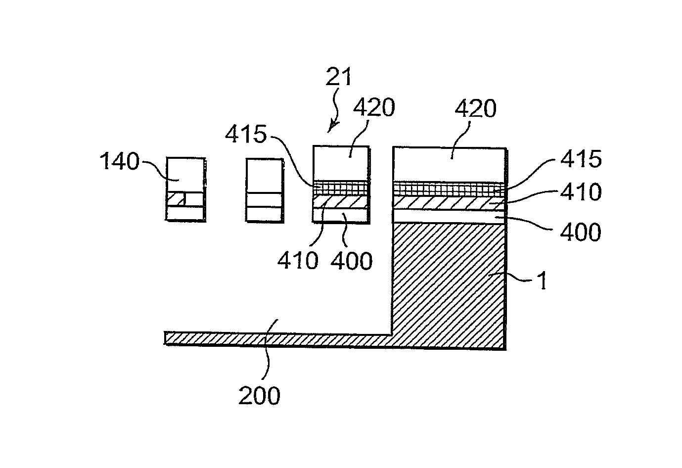
[0071]FIG. 11 is an enlarged partly sectional view of an infrared detecting device of the present embodiment and shows particularly a sectional structure (corresponding to a developed section of a spot cut along line X-Y of FIG. 1) of a beam portion 21. The beam portion 21 is provided, using an SOI substrate 1, over an embedded silicon oxide film 400 embedded therein and configured by a wiring corresponding to a laminated body of a silicon film 410 and a metal silicide 415 provided thereon, and a silicon nitride film 420 (protective film) provided thereon. The largest point of difference between the structure according to the present embodiment and the conventional structure in this case resides in that a silicide region exists inside the form of a beam portion to be described later in a conventional meth...


PUM


Abstract

An infrared detecting device is provided that is capable of improving device characteristics thereof by narrowing the width of each beam portion. The infrared detecting device has an infrared detection portion having a thermoelectric transducing part formed over a semiconductor substrate via an air gap interposed therebetween, and the beam portions which are formed over the semiconductor substrate via the air gap interposed therebetween, support the infrared detection portion and electrically connect between the infrared detection portion and the semiconductor substrate, wherein each of the beam portions has an insulating material film and a conductive material layer exposed from the insulating material film to a side surface of each beam portion.

Description

BACKGROUND OF THE INVENTION[0001]The present invention relates to an infrared detecting device and a manufacturing method thereof, and particularly to wiring structures of beam portions in a thermal-type infrared detecting device structure.[0002]A conventional infrared detecting element or device has made use of band-to-band transition of electrons with infrared absorption and has been called “quantum type”. In order to improve its detection sensitivity, there was a need to cool it to liquid nitrogen temperature or less and operate it in a state in which thermal noise has been eliminated. Therefore, the quantum type infrared detecting device essentially needs to have a chiller such as a stirling cooler. This is large in size and very expensive. Since its maintenance is also cumbersome in addition to the above, the infrared detecting device has been centered on applications to the field of military technology except for research work.[0003]Since the market publication of an entirely ...

Claims


Application Information

Patent Timeline
Patent Type & Authority Patents(United States)
IPC IPC(8): G01J5/00
CPCG01J5/02G01J5/023G01J5/20
Inventor INOMATA, DAISUKE
Owner LAPIS SEMICON CO LTD
Why Eureka
Try Eureka