Transistor resistor and associated method

a technology of resistor and resistor, which is applied in the direction of amplifiers with semiconductor devices only, amplifiers with semiconductor devices/discharge tubes, gain control, etc., can solve the problems of large resistance requirements of circuits, poor linearity, and huge challenges in modern ic design, and achieve good resistance linearity, high resistance, and high resistance.

Active Publication Date: 2012-05-15
REALTEK SEMICON CORP
View PDF1 Cites 4 Cited by
  • Summary
  • Abstract
  • Description
  • Claims
  • Application Information

AI Technical Summary

Benefits of technology

[0008]Yet another objective of the present invention is to provide a transistor resistor and an associated method where the transistor resistor has good resistance linearity and offers high resistance.

Problems solved by technology

However, some circuits require very large resistance.
This will create tremendous challenge in modern IC design where small-size, high-density IC is required.
But a big drawback of such approach is that the resistance will change along with input signals, hence resulting in poor linearity.

Method used


Image

  • Transistor resistor and associated method
  • Transistor resistor and associated method
  • Transistor resistor and associated method

Examples


Embodiment Construction

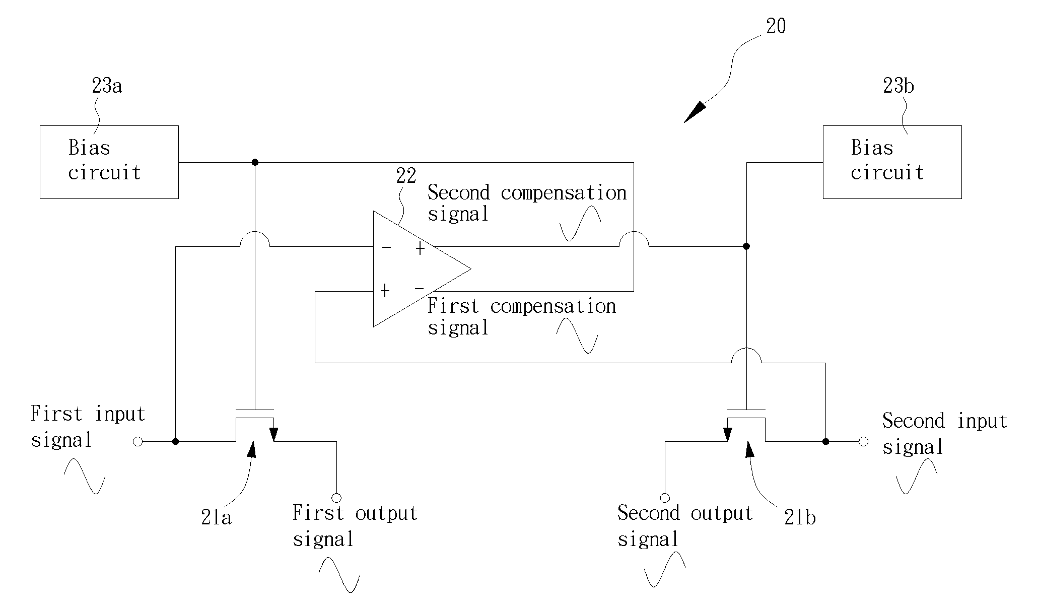
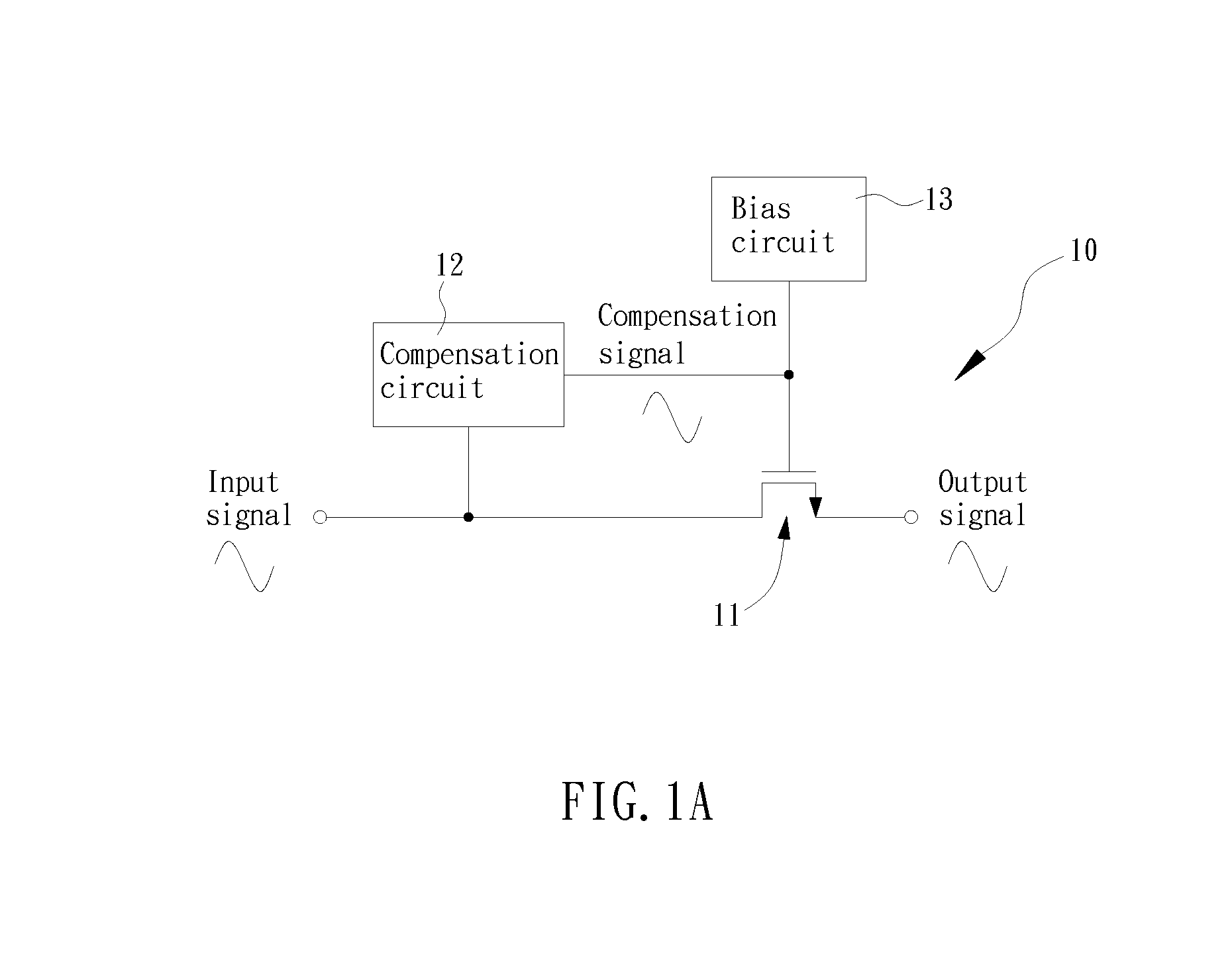
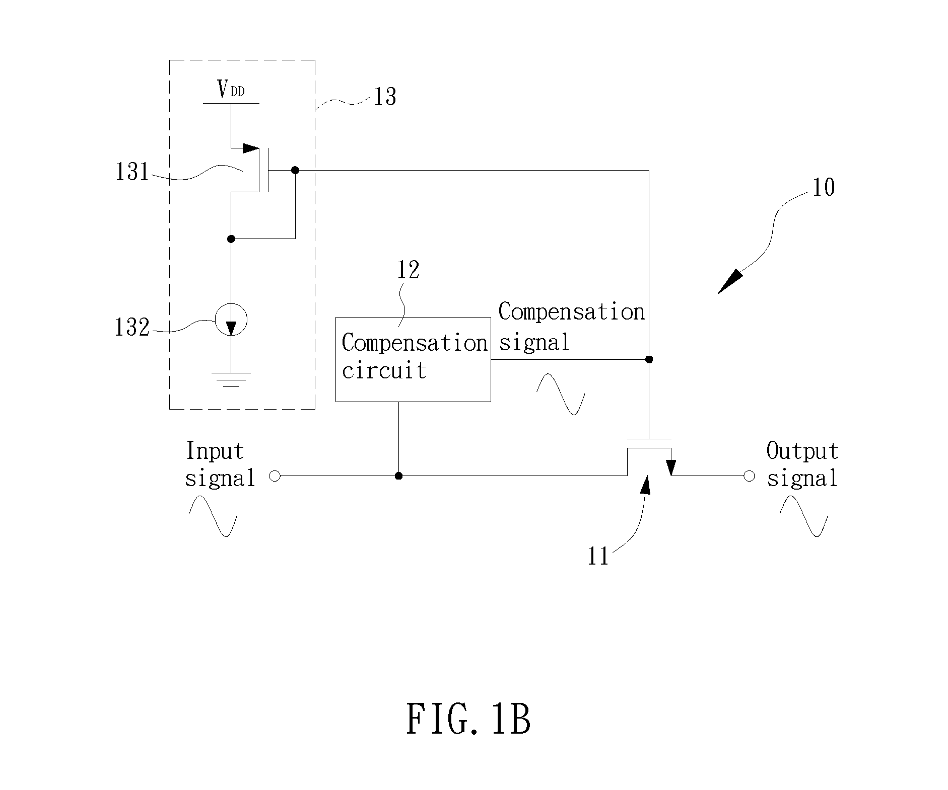
[0018]The description below will use a MOS transistor as an example, but the scope of the invention is not limited to the MOS transistor. FIG. 1A is a diagram of a transistor resistor according to an embodiment of the invention. As shown, the transistor resistor 10 comprises a NMOS transistor 11, a compensation circuit 12 and a bias circuit 13. The NMOS transistor 11 operates in the resistive region, that is, its gate-to-source voltage VGS must be greater than a threshold voltage VT, and its drain-to-source voltage VDS must be smaller. When the NMOS transistor 11 operates in resistive region, a current iD will flow into the drain and flow out of the source, and the relationship between iD and VDS is:

iD=2K(VGS−VT)VDS  Eq. (1)

[0019]where

[0020]K=12⁢μ⁢⁢Coxn⁢WL,

μn and Cox are material-specific parameters, and W and L are respectively the width and length of the gate. From Eq. (1), the resistance of the NMOS transistor 11 is derived as:

RMOS=VDS / iD=1 / [2K(VGS−VT)]  Eq. (2)

[0021]As shown in ...


PUM


Abstract

A transistor resistor and an associated method are provided to improve the resistance linearity of the transistor resistor. The transistor resistor includes a transistor operating in the resistive region, where the drain and source of the transistor receive an input signal and an output signal respectively. The transistor resistor also includes a compensating circuit for generating a compensating signal according to the input signal. The compensating signal is provided to the gate of the transistor such that the voltage difference between the gate and source of the transistor approximates to a constant.

Description

BACKGROUND OF THE INVENTION[0001](a). Field of the Invention[0002]This invention relates to a resistor device, and more particularly, to a transistor resistor and an associated method.[0003](b). Description of the Prior Arts[0004]Resistors are commonly used in integrated circuits (IC). Modern semiconductor processes offer several methods for resistor implementation. For example, the standard complimentary metal oxide semiconductor (CMOS) process provides several types of resistor, such as silicided polysilicon, silicided p+ or n+ active region, n-well and metal layer, where n-well has the highest resistance per unit area at about 1 k ohm / square. However, some circuits require very large resistance. For instance, a 3 dB 100 kHz first-order filter with 10 pF capacitance requires 160k ohm resistance, which means the resistor, even if a n-well resistor is used, will occupy a large space within the IC. This will create tremendous challenge in modern IC design where small-size, high-densi...

Claims


Application Information

Patent Timeline
Patent Type & Authority Patents(United States)
IPC IPC(8): H03F3/04
CPCH03H11/245
Inventor LIN, YING-YAO
Owner REALTEK SEMICON CORP
Why Eureka
Try Eureka