
Silicon single crystal pulling method

a single crystal and pull method technology, applied in the direction of crystal growth process, polycrystalline material growth, under a protective fluid, etc., can solve the problem of long time for the actual diameter of the silicon single crystal to approximate the set value, difficult to maintain the diameter of the cylindrical portion of the silicon single crystal constant, and difficult to accurately control the diameter of the silicon single crystal

Active Publication Date: 2012-05-29
SUMCO CORP
View PDF20 Cites 5 Cited by
  • Summary
  • Abstract
  • Description
  • Claims
  • Application Information

AI Technical Summary

Benefits of technology

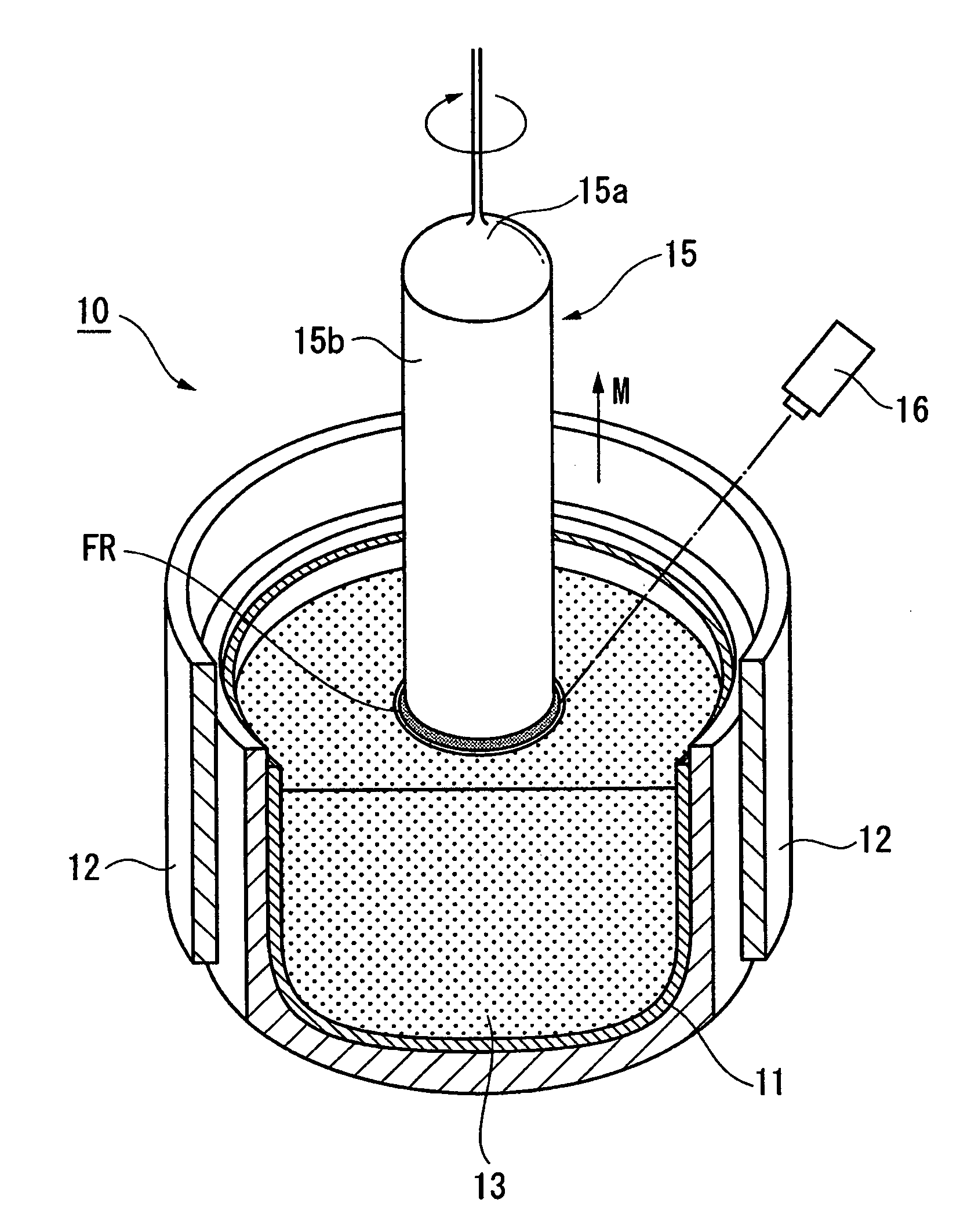
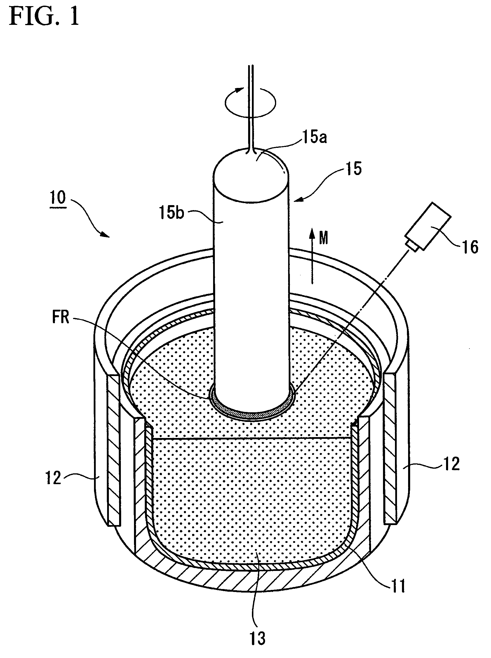
The present invention provides a method for pulling silicon single crystals with precise control over their diameter. This is achieved by measuring the brightness distribution of a fusion ring generated at the solid-liquid interface between the silicon melt and the silicon single crystal, and controlling the diameter of the silicon single crystal to match a predetermined value. This method ensures high-quality silicon wafers with minimal crystal defects, and reduces manufacturing costs by accurately controlling the diameter of the silicon single crystal.

Problems solved by technology

However, the above-mentioned method of measuring the diameter of the pulled silicon single crystal, calculating the difference between the measured value and the predetermined diameter value, and feeding back the difference makes it difficult to accurately control the diameter of the silicon single crystal.
That is, even though a diameter measuring position is set in the vicinity of a solid-liquid interface, it takes a long time for the actual diameter of the silicon single crystal to approximate the set value in the method of changing the temperature of the silicon melt or the pulling speed after a variation in the diameter of the silicon single crystal that has already been pulled up is detected.
Therefore, a wave occurs due to the variation in the diameter of the silicon single crystal, and it is difficult to maintain the diameter of the cylindrical portion of the silicon single crystal to be constant.
However, in the method of measuring the angle or diameter of the fusion ring which is regarded as an inclined plane and detecting the diameter of the silicon single crystal on the basis of the measured results, the interface of the fusion ring, which is a detection target, is unclear, and it is difficult to accurately detect the width or diameter of the fusion ring.
Therefore, it is difficult to feed back a variation in the width or diameter of the fusion ring to accurately control the diameter of the silicon single crystal.

Method used


Image

  • Silicon single crystal pulling method
  • Silicon single crystal pulling method
  • Silicon single crystal pulling method

Examples


examples

[0045]FIG. 4 is a graph illustrating the diameter of a silicon single crystal, a diameter variation (the differential value of the diameter), and the meniscus height of a silicon melt actually measured by the single crystal pulling apparatus. The measurement results shown in FIG. 4 proved that the variation in the diameter of the silicon single crystal and the meniscus height were substantially opposite to each other in phase.

[0046]FIG. 5 is a distribution chart illustrating the correlation between the variation in the diameter of the silicon single crystal and the meniscus height shown in FIG. 4. As can be seen from FIG. 5, when the diameter of the silicon single crystal is increased during the pulling process, the meniscus height is decreased. On the other hand, when the diameter of the silicon single crystal is decreased, the meniscus height is increased.

[0047]The single crystal pulling apparatus according to the related art inputs a diameter value, and performs a PID operation t...


PUM

PropertyMeasurementUnit
threshold percentaaaaaaaaaa
distanceaaaaaaaaaa
heightaaaaaaaaaa

Abstract

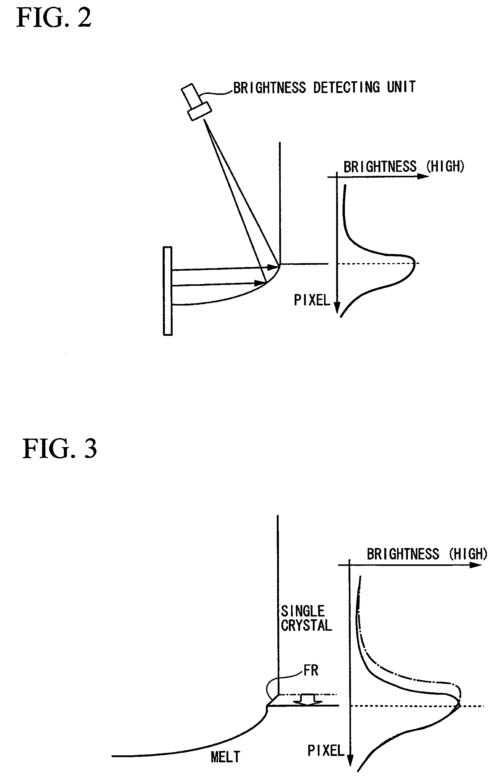
An object of the present invention is to provide a silicon single crystal pulling method of accurately controlling the diameter of a silicon single crystal, thereby obtaining a high-quality silicon single crystal with little crystal defect.According to an aspect of the present invention, the pulling step includes: capturing an image of the silicon single crystal using an imaging device; measuring the brightness distribution of a fusing ring generated in the vicinity of a solid-liquid interface between the silicon melt and the silicon single crystal for each image scan line in the image captured by the imaging device; detecting the liquid level of the silicon melt and the position of the solid-liquid interface; and controlling the diameter of the silicon single crystal on the basis of a meniscus height, which is a difference between the liquid level and the position of the solid-liquid interface.

Description

TECHNICAL FIELD[0001]The present invention relates to a silicon single crystal pulling method of accurately controlling the diameter of a silicon single crystal when the silicon single crystal is pulled up from a silicon melt by a Czochralski method, thereby obtaining a high-quality silicon single crystal with little crystal defect.BACKGROUND ART[0002]Various methods of manufacturing a silicon single crystal have been proposed. Among them, a Czochralski method (hereinafter, referred to as a CZ method) is the most common silicon single crystal manufacturing method. In the CZ method of growing a silicon single crystal, polysilicon is melted in a crucible to form a silicon melt. Then, a seed crystal is deposited to the silicon melt, and the seed crystal is pulled up at a predetermined rotational speed and a predetermined pulling speed to grow a cylindrical silicon single crystal below the seed crystal.[0003]A silicon wafer, which is a material forming a semiconductor device, is obtaine...

Claims


Application Information

Patent Timeline
Patent Type & Authority Patents(United States)
IPC IPC(8): C30B15/20
CPCC30B15/26H01L21/20
Inventor TAKANASHI, KEIICHI
Owner SUMCO CORP
Learn More