Method for producing layered product, layered product, method for producing layered product with device using said layered product, and layered product with device

a technology of layered products and products, applied in the direction of synthetic resin layered products, transportation and packaging, other domestic articles, etc., can solve the problems of warpage and exfoliation of thin films, unsatisfactory cases, and poor performance, and achieve easy releasability of parts, small defects, and precise positioning

Active Publication Date: 2018-02-20
TOYOBO CO LTD
View PDF18 Cites 1 Cited by
  • Summary
  • Abstract
  • Description
  • Claims
  • Application Information

AI Technical Summary

Benefits of technology

[0037]According to the present invention, since the polyimide layered product with the support is in a state of being supported by a support having heat resistance and rigidity, at the time of the circuit wiring preparation and the semiconductor formation, precise positioning can be performed to perform the preparation of multi-layered thin films, the circuit formation and the like, and thin film deposition and the like can be performed without peeling off the polyimide layered product from the support even in a high-temperature process at the time of the semiconductor formation. Furthermore, since the surface of the polyimide layered product on which the device preparation is performed is smooth, there are provided a polyimide layered product with a support used for the preparation of a high-performance device and for a polyimide layered product with a device on which a circuit with extremely little defects in wiring and a semiconductor element are formed, and a polyimide layered product with a support with a device.
[0038]Moreover, when a support is peeled off from a polyimide layered product with a device with the support on which this circuit and the semiconductor element are formed, since an easily releasable part can be easily peeled off in the case where only the easily releasable part in the pattern is peeled off, it is possible to provide a polyimide layered product with a device without breaking the prepared semiconductor.
[0039]At the time of performing precise positioning to perform the preparation of multi-layered thin films, the circuit formation and the like, on the circuit wiring preparation, when a shape variable polyimide film unsatisfactory in dimensional stability is used alone as the support, it becomes difficult to perform positioning for the device preparation. On the other hand, in a method of fixing a polyimide film to a rigid support excellent in dimensional stability and peeling off this rigid support after the device preparation, a layered product with which peeling between a polyimide film and a support can be smoothly performed and having a peel strength by which exfoliation is not caused at the time of passing the process has been required. This enables the conventional electronic device preparation process to be used as it is, and it is possible to stably perform the device preparation on a polyimide film with precision. Particularly, the polyimide layered product with the support according to the present invention is a layered product useful for the case where the circuit formation is performed at a high temperature and for the formation of a sophisticated circuit, and there is provided a polyimide layered product with a support in which a polyimide film after the formation of a circuit and the like can be easily peeled off from the support.
[0040]Moreover, although solar cells and the like made from single-crystal Si and polycrystalline Si have problems in handling during a process and in durability after their completion since they have become thin and are easily broken, the polyimide layered product with the support according to the present invention can also be utilized as a reinforced substrate prepared by bonding a polyimide film. In this case, since there is a part easily peeled off, a reinforced substrate capable of electrode drawing can be prepared.
[0041]Moreover, in the case where a polyimide varnish is applied to a support and then peeled off to prepare a polyimide film, there are problems that the concentric film thickness distribution is given on the polyimide film, the polyimide film suffers from warpage when peeled off because of the difference between the structures of front and back surfaces, and it is difficult to keep the physical properties of the polyimide film unchanged so as to maintain moderate peel strength. In contrast, in the case of bonding a film prepared separately as in the present invention, the uniformity of film thicknesses at the points within a narrow area on a wafer, a sheet of glass or the like is extremely high, and the case is suitable for the circuit preparation because either of previously forming a circuit and then bonding, and bonding and then forming a circuit is acceptable.

Problems solved by technology

Moreover, in the case where there is a scratch or the like on the surface, the case is not desirable because the scratch or the like causes disconnection of wiring.
Si has a coefficient of linear thermal expansion of approximately 3 ppm / ° C., and in the case where this thin film is deposited on a substrate, when the difference in the coefficient of linear thermal expansion between the substrate and the thin film is large, the stress accumulated in the thin film causes the deterioration in performance, and the warpage and exfoliation of the thin film.
Moreover, for forming a hydrogenated amorphous silicon thin film, there is a possibility that a substrate is heated at a temperature of approximately 200° C. to 300° C. In this case, even when a thermoplastic resin is used as the polymeric film, the performance is unsatisfactory.
However, since ceramic is not flexible and cannot be made thin, the applicable field is restricted.
Since these polyimide films generally have a large coefficient of linear thermal expansion, and have problems that the dimensional change caused by the change in temperature is significant and these films are not suitable for the production of a circuit having fine wiring, the applicable field is restricted.
As described above, a device including a polyimide film with physical properties satisfactory for a base material provided with heat resistance, high mechanical properties and flexibility has not yet been obtained.
Although these polyimide benzoxazole films made from a polyimide having a benzoxazole ring in the main chain have an improved tensile breaking strength, an improved tensile elastic modulus, and a satisfactory coefficient of linear thermal expansion, in contrast to their excellent mechanical properties, the thinner the film is, the more difficult it is to be handled.
Accordingly, these films still have problems that they are insufficient from mechanical and dynamical aspects, and the like.
Although a polyimide having a biphenyl structure in the main chain also has an improved tensile breaking strength, an improved tensile elastic modulus, and a satisfactory coefficient of linear thermal expansion, in contrast to its excellent mechanical properties, the thinner the polyimide film is, the more difficult it is to be handled.
Accordingly, the polyimide film still has problems that it is insufficient from mechanical and dynamical aspects, and the like.
However, with regard to polysilicon, an oxide semiconductor, and the like, in the case where a process in a temperature range of approximately 200 to 500° C. is required, no method is known in which an adhesive agent or a tackiness agent for bonding use having a sufficient resistance for practical use is employed.
Moreover, since the conventional thermoplastic resin generally has a large coefficient of linear thermal expansion and there is a limit for making this layer thin, as compared to a polyimide film and a substrate made from an inorganic substance, an adhesive layer made of a thermoplastic resin and the like has a tendency to adversely affect the dimensional stability in a heating process.
However, at the time of peeling, since laser radiation to an adhesive agent layer is performed and etching means is used, the process is complicated and requires high production costs.
Therefore, the film excellent in productivity is difficult to be used for the device.
Moreover, in the case where a film free from a slip agent is transported by many rolls, the film inevitably suffers from fine scratches during the process.
As such, except to apply a varnish free from a slip agent directly to a glass substrate or the like and bake the coating film, it has been difficult to prepare a smooth surface.

Method used


Image

  • Method for producing layered product, layered product, method for producing layered product with device using said layered product, and layered product with device
  • Method for producing layered product, layered product, method for producing layered product with device using said layered product, and layered product with device
  • Method for producing layered product, layered product, method for producing layered product with device using said layered product, and layered product with device

Examples


examples

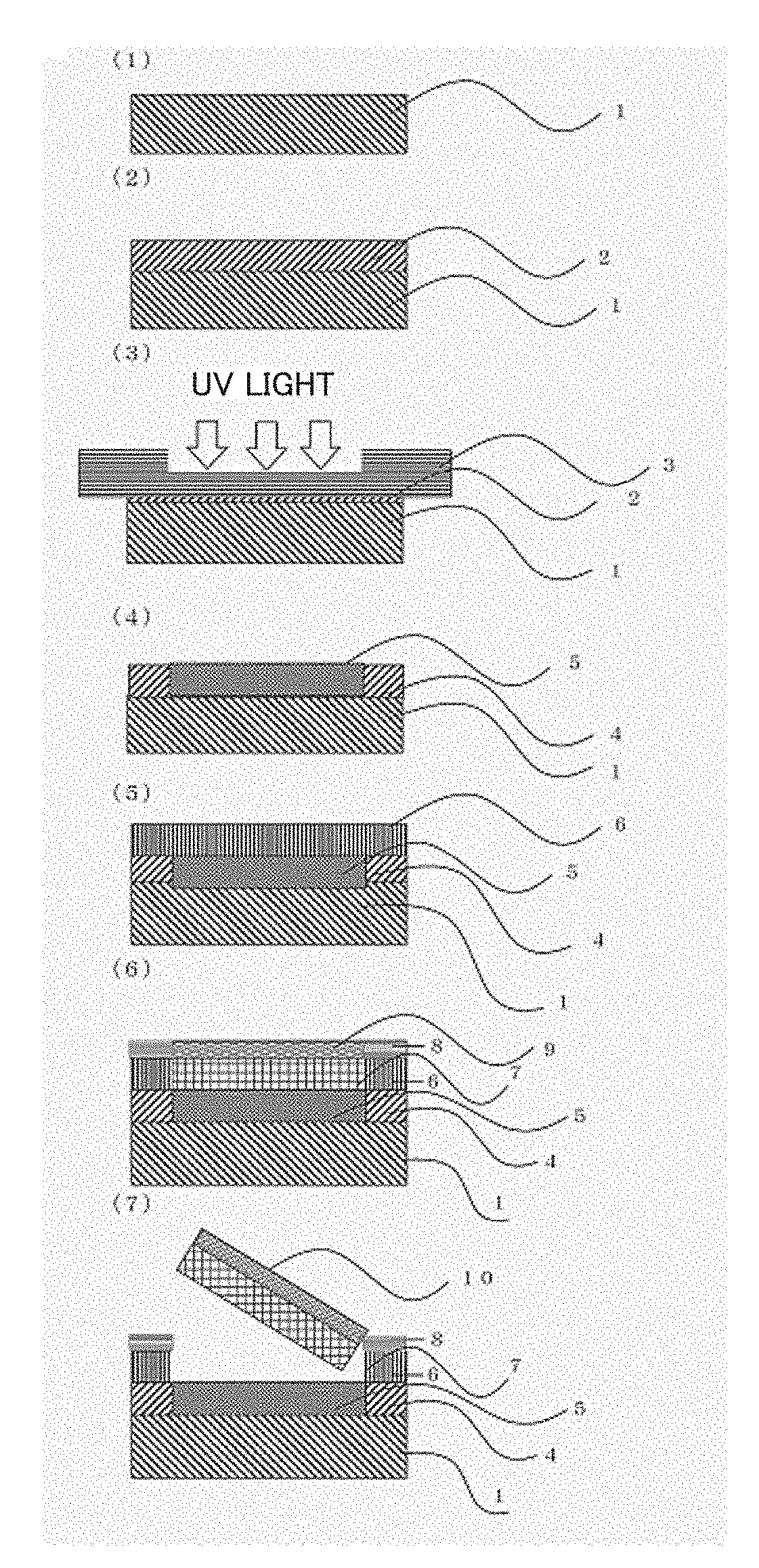
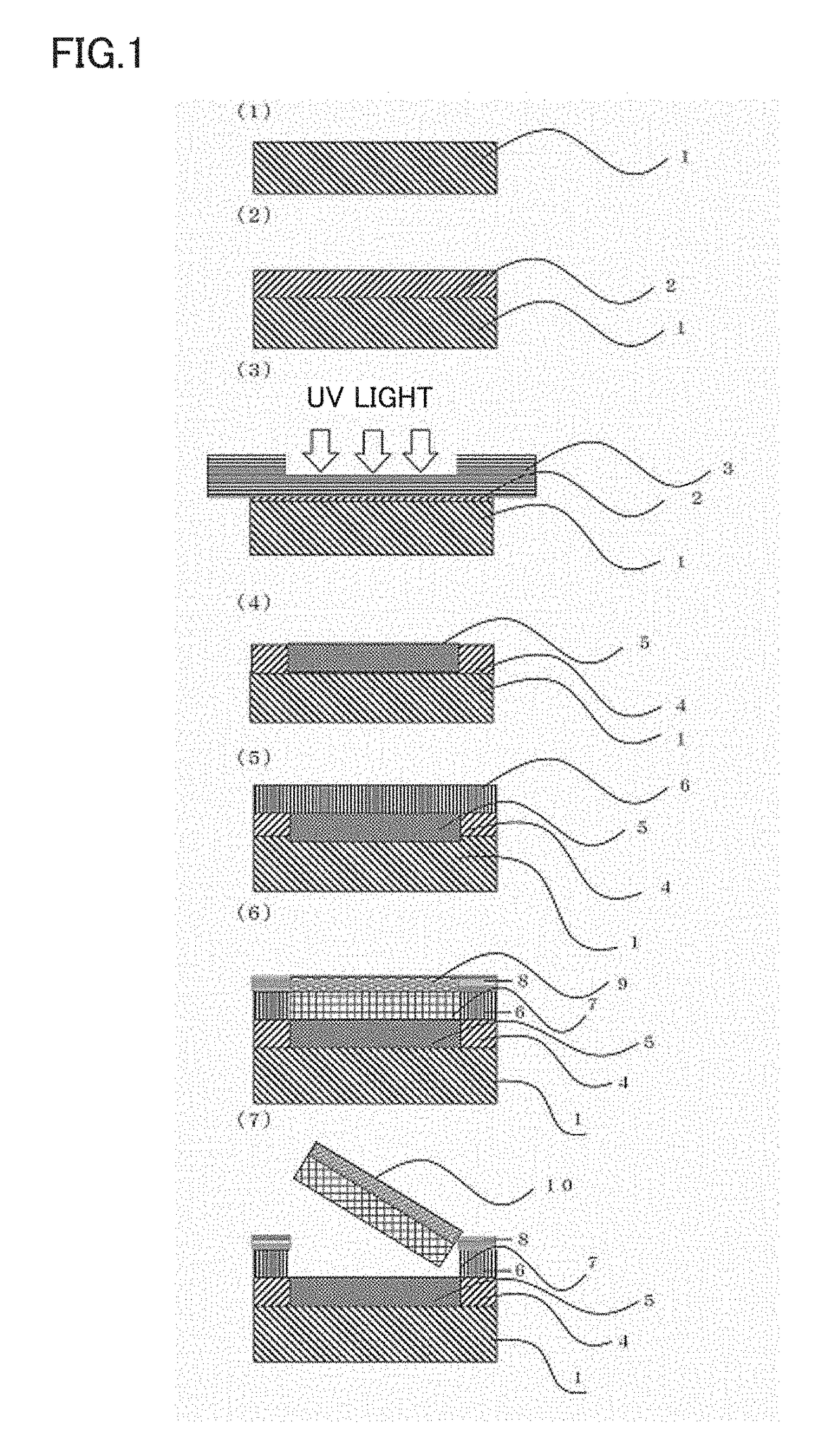
[0145]Hereinafter, the present invention will be described in more detail with reference to examples and comparative examples, but the present invention is not limited by the following examples. In this connection, the methods of evaluating physical properties in the following examples are as follows.

1. Reduced Viscosity of Polyamic Acid (ηsp / C)

[0146]A solution prepared by dissolving a polymer in N-methyl-2-pyrrolidone (or N,N-dimethylacetamide) so that the polymer concentration became 0.2 g / dl was measured at 30° C. with an Ubbelohde type viscosity tube (in the case where the solvent used for the preparation of the polyamic acid solution was N,N-dimethylacetamide, a polymer was dissolved in N,N-dimethylacetamide and the reduced viscosity was measured).

2. Solution Viscosity of Polyamic Acid Solution

[0147]The solution viscosity was measured at 25° C. with a Brookfield viscometer.

3. Thickness of Polyimide Film or the Like

[0148]The thickness was measured using a micrometer (available f...

production examples 1 to 3

(Preparation of Polyamic Acid Solution A)

[0184]After the inside of a reaction vessel equipped with a nitrogen inlet tube, a thermometer and a stirring rod was replaced with nitrogen, 223 parts by mass of 5-amino-2-(p-aminophenyl)benzoxazole and 4416 parts by mass of N,N-dimethylacetamide were added thereto and completely dissolved. Then, 217 parts by mass of pyromellitic acid dianhydride and SNOWTEX prepared by dispersing colloidal silica as a slip agent in dimethylacetamide (DMAC-ST30, available from Nissan Chemical Industries, Ltd.) in an amount that the silica content becomes the content described in Table 1 were added thereto. The liquid was stirred for 24 hours at a reaction temperature of 25° C., whereupon each of brown viscous polyamic acid solutions A1 to A3 was obtained. The measurement results are described in Table 1 and Table 2.

production examples 4 to 6

(Preparation of Polyamic Acid Solution B)

[0185]After the inside of a reaction vessel equipped with a nitrogen inlet tube, a thermometer and a stirring rod was replaced with nitrogen, 398 parts by mass of 3,3′,4,4′-biphenyltetracarboxylic acid dianhydride as a tetracarboxylic acid dianhydride and 147 parts by mass of paraphenylenediamine were dissolved in 4600 parts by mass of N,N-dimethylacetamide. The solution was subjected to a reaction in the same manner while the temperature was maintained at a temperature less than or equal to 20° C. to obtain each of polyamic acid solutions B1 to B3. The measurement results are described in Table 1 and Table 2.


PUM

PropertyMeasurementUnit
temperatureaaaaaaaaaa

Abstract

By preparing a polyimide film with a face at the support side and subjected to a surface treatment; subjecting at least one of a face of the support and the face of the polyimide film which are opposite to each other to a patterning treatment using a coupling agent to form a satisfactorily bondable part and an easily releasable part which differ in adhesion / peel strength; subsequently, superposing the support and the polyimide film to be subjected to a pressurizing / heating treatment and to be bonded to each other, subjecting the surface of the polyimide film to an organic alkali treatment; and then, applying a polyamic acid solution free from a slip agent ingredient, drying the coating film and imidizing the film, a layered product having a structure of at least three layers in which at least one layer contains a slip agent material and both surface layers have no slip agent material is produced.

Description

CROSS-REFERENCE TO RELATED APPLICATIONS[0001]This patent application is the U.S. national phase of International Patent Application No. PCT / JP2013 / 066194, filed Jun. 12, 2013, which claims the benefit of Japanese Patent Application No. 2012-138754, filed on Jun. 20, 2012, and Japanese Patent Application No. 2012-257656, filed on Nov. 26, 2012, which are incorporated by reference in their entireties herein.TECHNICAL FIELD[0002]The present invention relates to a method for producing a polyimide layered product with a support including the polyimide layered product and the support, and the polyimide layered product with the support. In addition, the present invention relates to a method for producing a polyimide layered product with a device with a support prepared by forming the device on the polyimide layered product with the support, and the polyimide layered product with the device with the support, and relates to a method for producing a polyimide layered product with a device pre...

Claims


Application Information

Patent Timeline
Patent Type & Authority Patents(United States)
IPC IPC(8): B32B3/10B32B5/14B32B27/08B32B37/00B32B38/10H05K3/00B32B27/28B32B7/06B32B37/12B32B27/36B32B27/16H05K1/03B32B38/04B32B37/18
CPCB32B27/281B32B7/06B32B27/08B32B27/16B32B27/36B32B37/0038B32B37/12B32B38/10H05K3/007B32B5/145Y10T428/24612B32B37/182B32B38/04B32B2250/04B32B2255/10B32B2255/26B32B2307/746B32B2307/748B32B2310/0831B32B2379/08B32B2457/00B32B2457/08B32B2457/14H05K1/0346H05K2201/0154B32B37/26
Inventor NAKASE, KATSUKIOKUYAMA, TETSUOTSUCHIYA, TOSHIYUKIMAEDA, SATOSHIOUYA, KAZUYUKI
Owner TOYOBO CO LTD
Why Eureka
Try Eureka