Supercharge Your Innovation With Domain-Expert AI Agents!

Method for manufacturing semiconductor device having a dual gate insulation layer

a technology of gate insulation layer and semiconductor, applied in the direction of semiconductor devices, basic electric elements, electrical appliances, etc., can solve the problems of increasing the loss of isolation layer, prone to being easily etched, and the unwanted characteristics of the insulation layer, so as to reduce the formation of steps and stabilize the characteristics of the gate insulation layer

Inactive Publication Date: 2012-05-29
SK HYNIX INC
View PDF9 Cites 0 Cited by
  • Summary
  • Abstract
  • Description
  • Claims
  • Application Information

AI Technical Summary

Benefits of technology

The present invention provides a method for manufacturing a semiconductor device that can prevent defects in the semiconductor substrate and improve the characteristics and reliability of the semiconductor device. The method includes selectively removing a portion of an insulation layer formed on the semiconductor substrate and forming a second insulation layer on the first insulation layer and the semiconductor substrate in the first and second regions of the semiconductor substrate. The method also includes sequentially forming a conductive layer and a hard mask layer on the second insulation layer and forming gates in the first and second regions of the semiconductor substrate by etching the hard mask layer, conductive layer, and insulation layers. The method can stabilize the characteristics of the gate insulation layer and improve the reliability of the semiconductor device.

Problems solved by technology

However, in the conventional method for forming a dual gate insulation layer, when conducting a wet etching process for selectively removing the gate insulation layer in the peripheral region, not only the gate insulation layer in the peripheral region is removed, but also unwanted losses to the isolation layer result in a step portion when formed between an active region and the isolation layer.
Unfortunately, the resultant SOD insulation layer exhibits unwanted characteristics in that the SOD insulation layer is prone to being easily etched when conducting wet etching processes.
As a result, losses of the isolation layer markedly increase and the thickness of a step portion increases up to 350 Å.
If the step portion is formed between the active region and the isolation layer due to the loss of the isolation layer, then the characteristics of the gate insulation layer become unstable.
Because of these facts, defects are likely to occur in a semiconductor substrate and the performance characteristics and reliability of a semiconductor device can deteriorate.

Method used


Image

  • Method for manufacturing semiconductor device having a dual gate insulation layer
  • Method for manufacturing semiconductor device having a dual gate insulation layer
  • Method for manufacturing semiconductor device having a dual gate insulation layer

Examples


Embodiment Construction

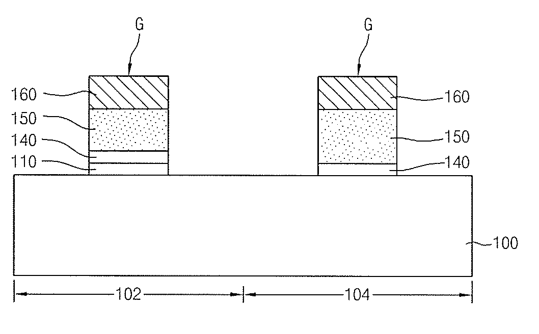
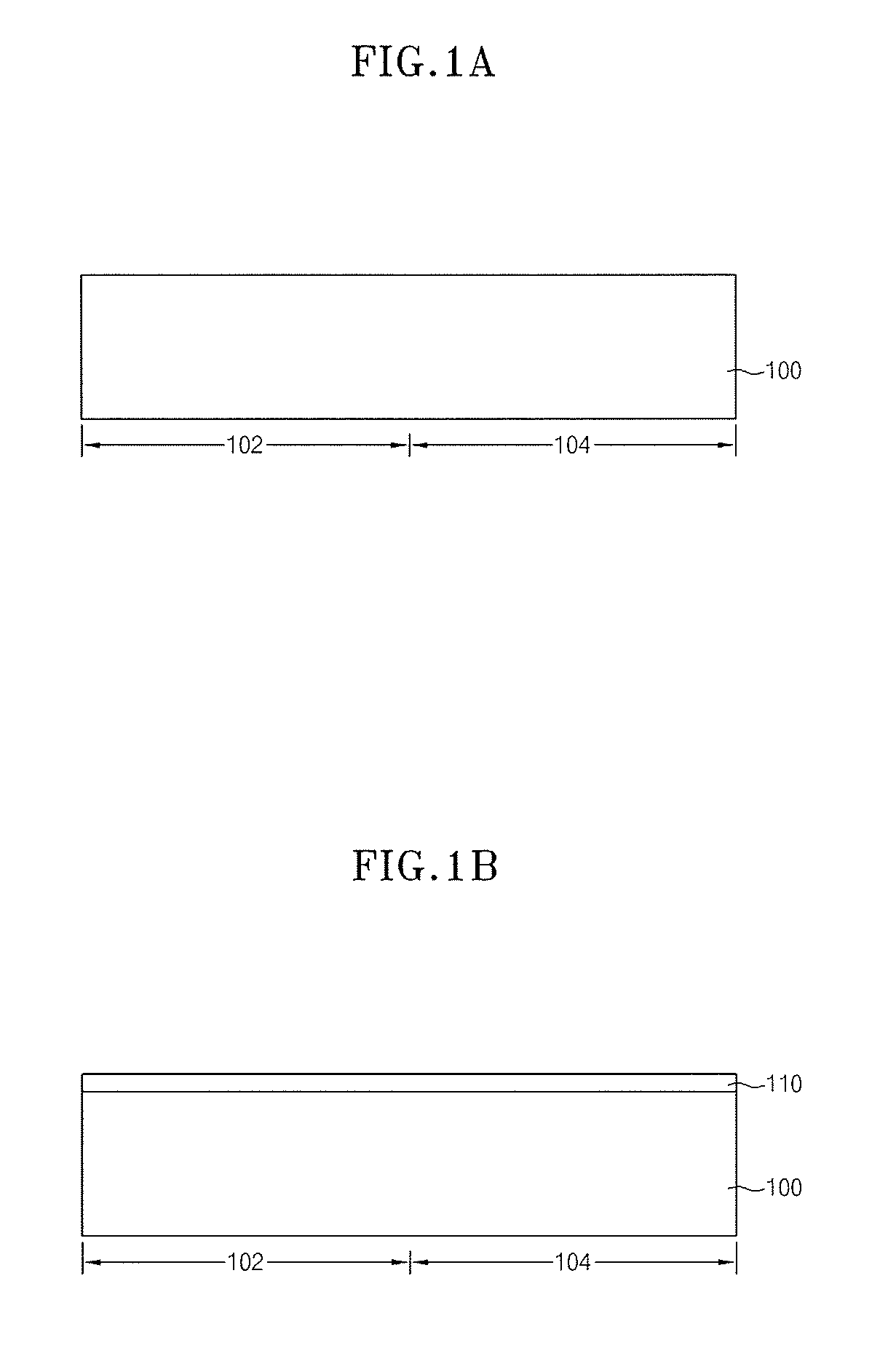
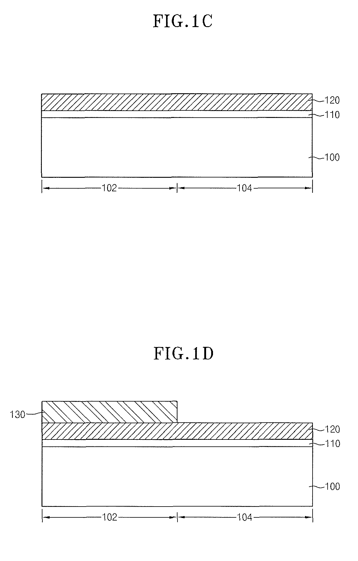
[0029]In an embodiment of the present invention, in order to form a dual gate insulation layer which has a relatively large thickness in a cell region and a relatively small thickness in a peripheral region, a portion of a gate insulation layer in the peripheral region is selectively removed by conducting a wet etching process using an etching solution composed of propylene glycol, HF (hydrofluoric acid) and amine.

[0030]Since the etching solution composed of propylene glycol, HF and amine has a low etching selectivity towards an oxide layer, to the loss of an isolation layer that is caused in the wet etching process can be reduced and step formation between an active region and the isolation layer can be lessened in this embodiment.

[0031]Conventional fabrication techniques often times use a wet etching process that employs a buffered oxide etchant (BOE) solution which has a high etching selectivity for an oxide layer to perform wet etching. The BOE solution not only etches gate insu...


PUM


Abstract

A method for manufacturing a semiconductor device having a dual gate insulation layer is presented. The method includes a step of forming a first insulation layer on a semiconductor substrate which has a first region and a second region. The method includes a step of selectively removing a portion of the first insulation layer formed the second region of the semiconductor substrate. The removal of the portion of the first insulation layer is conducted using an etching solution comprising propylene glycol, HF and amine. The method also includes a step of forming a second insulation layer on the first insulation layer in the first region and on the semiconductor substrate in the second region.

Description

CROSS-REFERENCE TO RELATED APPLICATIONS[0001]The present application claims priority to Korean patent application number 10-2009-0031416 filed on Apr. 10, 2009, which is incorporated herein by reference in its entirety.BACKGROUND OF THE INVENTION[0002]The present invention relates to a method for manufacturing a semiconductor device, and more particularly, to a method for manufacturing a semiconductor device which can lessen step formation due to unwanted losses of an isolation layer and thereby stabilize the characteristics of a gate insulation layer.[0003]Generally gate insulation layers in semiconductor devices are grown through annealing or rapid thermal annealing processes that produce a silicon oxide layer (an SiO2 layer). As the design rules demand more diminutive semiconductor devices, the thickness of the gate insulation layer is reduced down to a thickness level that defines a tunneling limit.[0004]Due to the refresh characteristics of transistors in a cell region, the tra...

Claims


Application Information

Patent Timeline
Patent Type & Authority Patents(United States)
IPC IPC(8): H01L21/8234
CPCH01L21/31111H01L21/823462Y10S438/981H01L21/18
Inventor LEE, YOUNG BANG
Owner SK HYNIX INC
Features
  • R&D
  • Intellectual Property
  • Life Sciences
  • Materials
  • Tech Scout
  • Unparalleled Data Quality
  • Higher Quality Content
  • 60% Fewer Hallucinations
Learn More