Optical system

a technology of optical systems and optical components, applied in the field of optical systems, can solve the problems of difficult to achieve the miniaturization of the whole size, the ineffective reduction of the whole etc., and achieve the effect of reducing the size of the optical system

Active Publication Date: 2012-05-29
HIMAX TECH LTD
View PDF6 Cites 5 Cited by
  • Summary
  • Abstract
  • Description
  • Claims
  • Application Information

AI Technical Summary

Benefits of technology

[0008]Accordingly, the present invention is directed to an optical system, in which a whole size of the optical system can be effectively reduced.
[0020]According to the above descriptions, in the optical system of the present invention, the focusing motor can be disposed between the WLO lens module and the photo sensor or between the WLO lenses, so that a size of the focusing motor is relatively reduced to cope with the size of the WLO lens module, and therefore a whole size of the optical lens can be reduced. Moreover, since the focusing motor is disposed between the WLO lens module and the photo sensor or between the WLO lenses, during imaging, the optical system may have a [[zoom]]ing function and a focusing function, and an image light can be imaged on the photo sensor, optimally. In other words, the optical system of the present invention not only has a relatively small size, but also has a good optical imaging quality.

Problems solved by technology

However, a whole size of the optical system 100 cannot be effectively reduced due to such a structure, so that miniaturization of the whole size is hard to be achieved.

Method used


Image

  • Optical system
  • Optical system
  • Optical system

Examples


Embodiment Construction

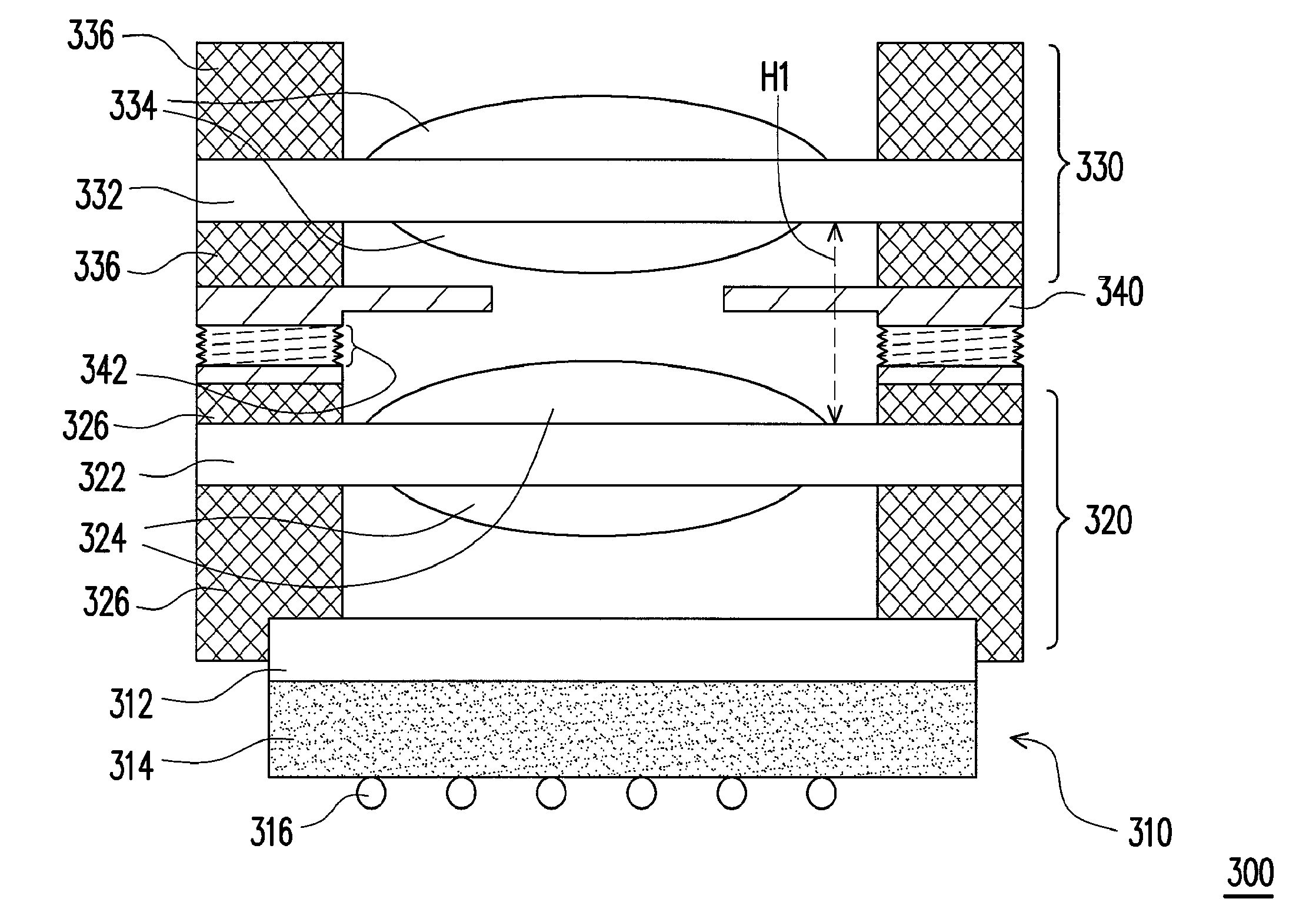
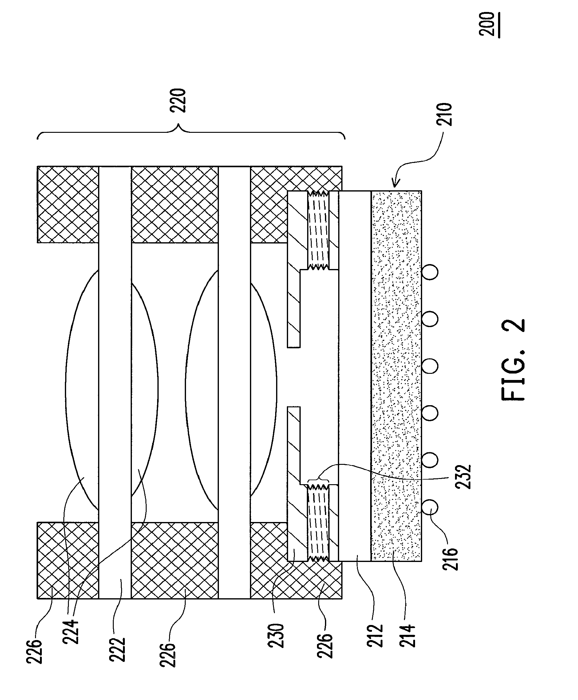
[0026]FIG. 2 is a schematic diagram of an optical system according to an embodiment of the present invention. Referring to FIG. 2, the optical system 200 of the present embodiment includes a photo sensor 210, a wafer level optical (WLO) lens module 220 and a focusing motor 230. In the present embodiment, the photo sensor 210 can be a complementary metal oxide semiconductor (CMOS) sensor or a charge coupled device (CCD), and the photo sensor 210 includes a cover glass 212, a photo sensor device substrate 214 and a plurality of tin balls 216. The cover glass 212 covers the photo sensor device substrate 214, and the tin balls 216 are electrically connected to the photo sensor device substrate 214.

[0027]The WLO lens module 220 is located on the photo sensor 210, and includes at least one transparent substrate 222 and at least one lens 224, wherein the at least one lens 224 is disposed on the at least one transparent substrate 222, as that shown in FIG. 2. In the present embodiment, the ...


PUM


Abstract

An optical system including a photo sensor, a wafer level optical (WLO) lens module and a focusing motor is provided. The WLO lens module is located at the photo sensor. The WLO lens module includes at least one transparent substrate and at least one lens, wherein the lens is disposed on the transparent substrate. The focusing motor is located between the WLO lens module and the photo sensor. The focusing motor drives the WLO lens module to move toward or backward the photo sensor.

Description

BACKGROUND OF THE INVENTION[0001]1. Field of the Invention[0002]The present invention relates to an optical system. More particularly, the present invention relates to an optical system.[0003]2. Description of Related Art[0004]As electronic products have a general trend of miniaturization and low price, a wafer level module (WLM) technique is disclosed. The WLM technique is mainly to fabricate the electronic product according to a wafer level fabrication technique, so as to miniaturize a size of the electronic product and reduce a cost thereof. Wherein, the WLM technique can also be applied for fabricating an optical system, so that a size of the optical system can be reduced compared to that of a conventional optical system, and accordingly the miniaturized optical system can be applied to, for example, a camera module of a mobile phone.[0005]FIG. 1 is a schematic diagram of a conventional optical system. Referring to FIG. 1, the optical system 100 includes a photo sensor 110, an o...

Claims


Application Information

Patent Timeline
Patent Type & Authority Patents(United States)
IPC IPC(8): G03B3/10G03B17/00
CPCG02B13/0085G02B13/009G03B3/10
Inventor CHEN, CHENG-HENG
Owner HIMAX TECH LTD
Why Eureka
Try Eureka