Method for producing a multi-beam deflector array device having electrodes

a technology of array devices and beams, which is applied in the direction of mass spectrometers, particle separator tubes, radiation therapy, etc., can solve the problems of not being able to meet the requirements of electrodes, electrodes are very sensitive to deformation and stress, and the production method is not expensive. , to achieve the effect of low cost and high functionality

Active Publication Date: 2012-06-12
IMS NANOFABTION
View PDF10 Cites 87 Cited by
  • Summary
  • Abstract
  • Description
  • Claims
  • Application Information

AI Technical Summary

Benefits of technology

[0011]The present invention sets out to present a method of producing said multi-beam deflector array means of high functionality at low cost.

Problems solved by technology

There are several problematic issues in the use of pattern definition devices as described in prior art: The shielding of the blanking apertures against cross-talking, for instance, as well as a non-expensive way of producing said blanking means.
In particular the forming of the electrodes employing perpendicular growth is a rather complex process.
Additionally, such electrodes are very sensitive to deformation and stress.
Moreover, electrodes that have a substantial height over the blanking plate impose a limitation of the electric field strength tolerable in the vicinity of the blanking plate (this is due to stray fields around the electrodes caused by the boundary conditions for the field lines).
This represents a disadvantage, especially when the blanking plate is used as a part of a grid lens (as for example described in U.S. Pat. No. 5,801,388 and U.S. Pat. No. 6,326,632 by the applicant / assignee) where the side of the blanking plate comprising the electrodes is used to define the electrostatic potential of the negative (diverging) and / or positive (collecting) electrostatic lens.

Method used


Image

  • Method for producing a multi-beam deflector array device having electrodes
  • Method for producing a multi-beam deflector array device having electrodes
  • Method for producing a multi-beam deflector array device having electrodes

Examples


Embodiment Construction

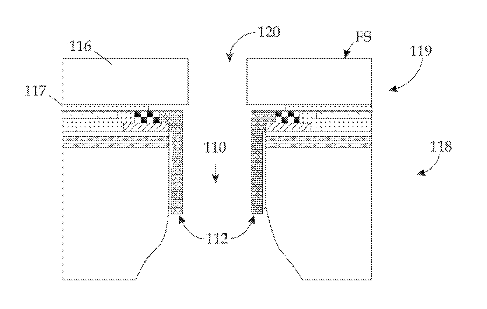
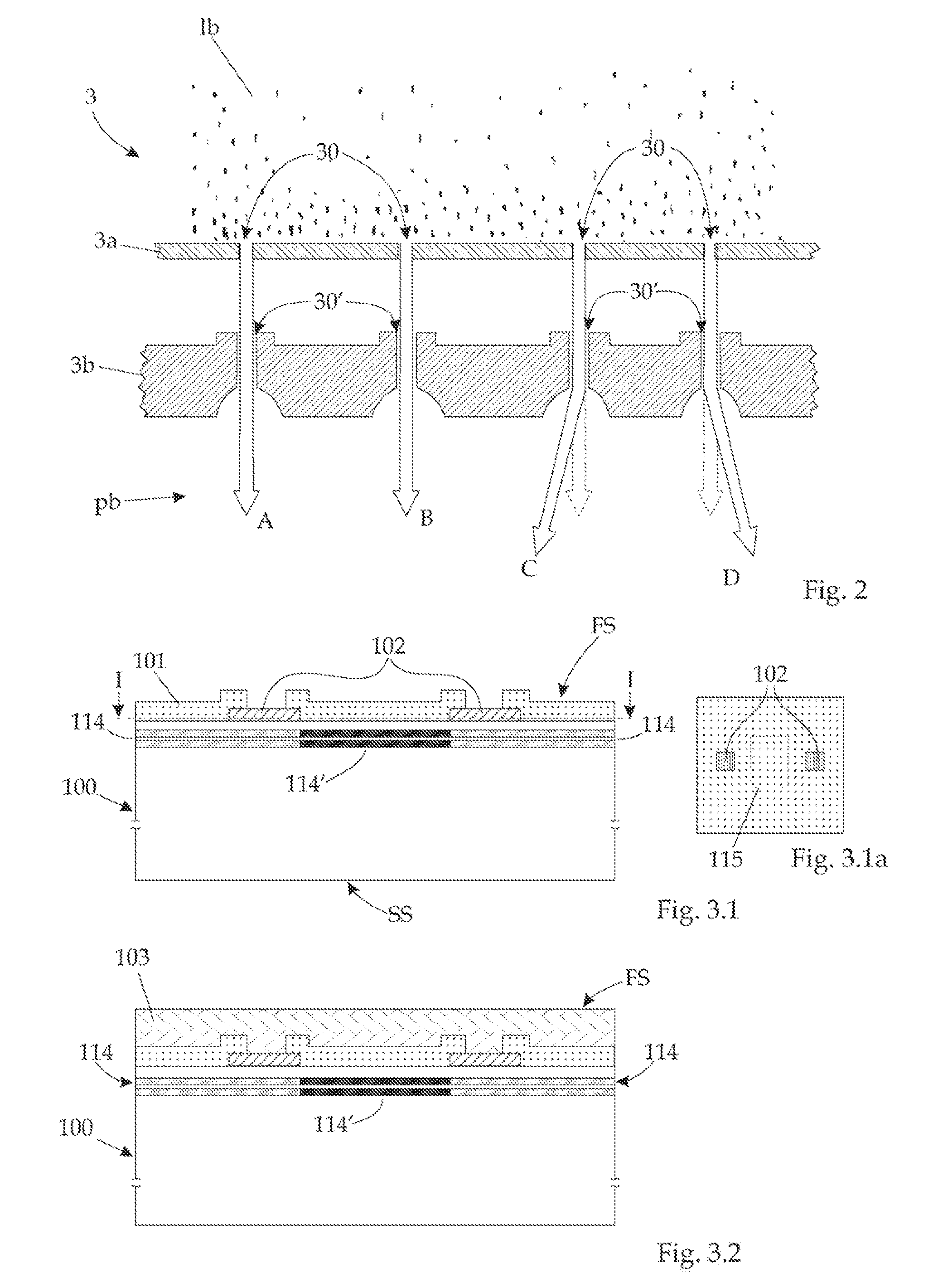
[0042]The preferred embodiments of the invention discussed in the following are related to a PML2-type particle-beam exposure apparatus with a pattern definition system as disclosed in the U.S. Pat. No. 6,768,125 and U.S. Pat. No. 7,276,714 of the applicant / assignee, and with a large-reduction projection system. In the following, first the technical background of the apparatus is discussed—as far as relevant to the invention—, then the invention is presented in detail.

[0043]It should be appreciated that the invention is not restricted to the following embodiments or the particular layout of the PD system, which merely represent one of the possible applications of the invention; the invention is suitable for other types of processing systems that employ a particle-beam with projector stages as well.

Maskless Particle-Beam Processing Apparatus

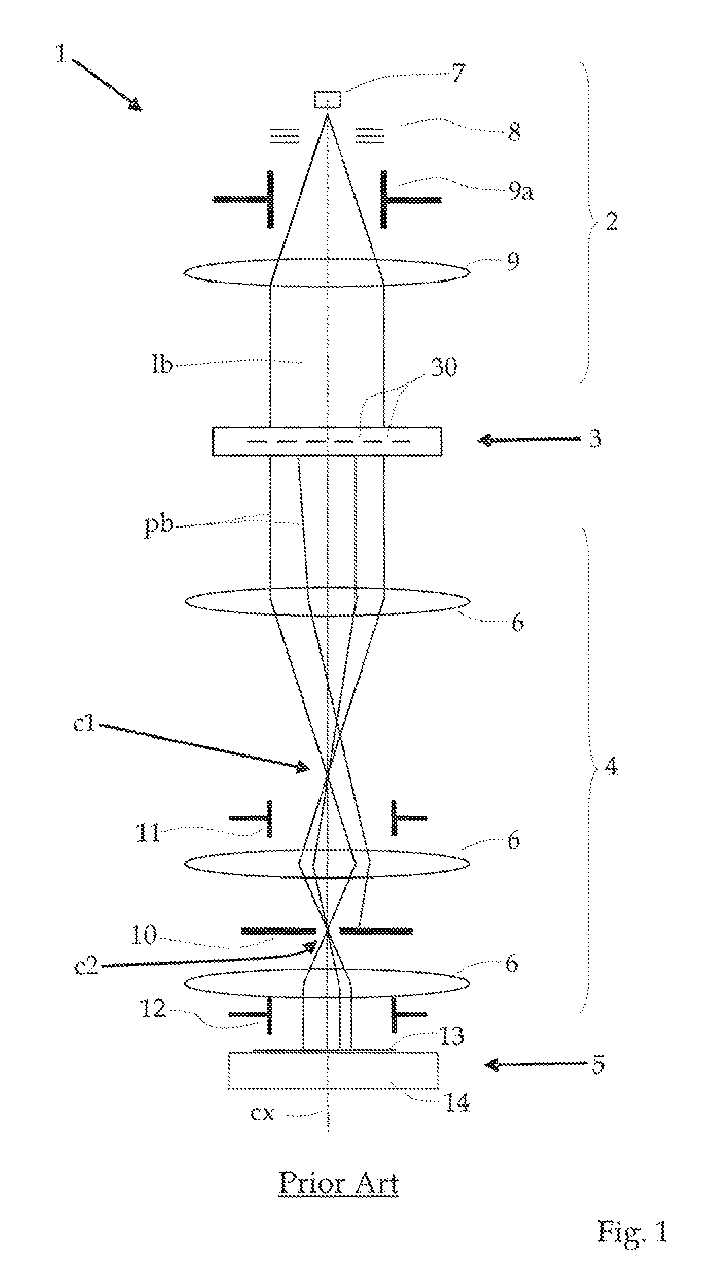
[0044]FIG. 1 shows a schematic overview of a maskless particle-beam processing apparatus PML2 which itself is known from prior art but is suitabl...


PUM


Abstract

The disclosure relates to a method for producing a multi-beam deflector array device with a plurality of openings for use in a particle-beam exposure apparatus, in particular a projection lithography system, said method starting from a CMOS wafer and comprising the steps of generating at least one pair of parallel trenches on the first side of the wafer blank at the edges of an area where the circuitry layer below is non-functional, the trenches reaching into the layer of bulk material; passivating the sidewalls and bottom of the trenches; depositing a conducting filling material into the trenches, thus creating columns of filling material serving as electrodes; attaching metallic contact means to the top of the electrodes; structuring of an opening between the electrodes, said opening stretching across abovementioned area so that the columns are arranged opposite of each other on the sidewalls of the opening.

Description

FIELD OF THE INVENTION AND DESCRIPTION OF PRIOR ART[0001]The present invention relates to a method for producing a multi-beam deflector array device with a plurality of openings for use in a particle-beam exposure apparatus, in particular a projection lithography system, starting from a CMOS wafer. The term “CMOS wafer” here stands for a silicon wafer having, on a first side, a circuitry layer beneath a contact layer and a cover layer serving as passivation layer. The CMOS circuitry is arranged in a suitable way so that electrical stray fields, which may be caused by the supply voltages or active elements (e.g. flip-flops) during operation, are shielded with respect to areas outside the CMOS layer.[0002]Furthermore, the invention relates to a multi-beam deflector array device for use in a particle-beam exposure apparatus produced with the abovementioned method.[0003]In a particle-beam exposure apparatus, a particle beam is generated and formed by an illumination system and illuminat...

Claims


Application Information

Patent Timeline
Patent Type & Authority Patents(United States)
IPC IPC(8): H01J37/147
CPCH01J37/045H01J37/3026H01J37/09H01J2237/0437
Inventor PLATZGUMMER, ELMARFRAGNER, HEINRICH
Owner IMS NANOFABTION
Why Eureka
Try Eureka