Dielectric deposition and etch back processes for bottom up gapfill

a technology of etching back and dielectric deposition, which is applied in the direction of basic electric elements, semiconductor/solid-state device manufacturing, electric apparatus, etc., can solve the problems of increasing the aspect ratio, affecting the operation of the completed device, and progressively more difficult to fill the gaps without leaving voids, so as to reduce the stress level of the dielectric layer and reduce film cracking

Active Publication Date: 2012-07-31
APPLIED MATERIALS INC
View PDF287 Cites 41 Cited by
  • Summary
  • Abstract
  • Description
  • Claims
  • Application Information

AI Technical Summary

Benefits of technology

[0007]Embodiments of the invention include methods to reduce film cracking in a dielectric layer. The methods may include the steps of depositing a first dielectric film on a substrate and removing a top portion of the first dielectric film by performing an etch on the film. The methods may also include depositing a second dielectric film over the etched first film, and removing a top portion of the second dielectric film. In addition, the methods may include annealing the first and second dielectric films to form the dielectric layer, where the removal of the top portions from the first and the second dielectric films reduces a stress level in the dielectric layer.
[0009]Embodiments still further include additional methods to reduce film cracking in a dielectric layer. The methods may include depositing a first dielectric film on a substrate and performing a first anneal on the first film. The methods may also include removing a top portion of the annealed first film by performing a first etch on the first film, and depositing a second dielectric film over the etched first film. In addition, the methods may include removing a top portion of the second dielectric film by performing a second etch on the second film, and performing a second anneal of the first and second dielectric films and forming the dielectric layer. The removal of the top portions from the first and the second dielectric films reduces a stress level in the dielectric layer.

Problems solved by technology

One of the persistent challenges faced in the development of semiconductor technology is the desire to increase the density of circuit elements and interconnections on substrates without introducing spurious interactions between them.
As circuit densities increase, however, the widths of these gaps decrease, increase their aspect ratios and making it progressively more difficult to fill the gaps without leaving voids.
The formation of voids when the gap is not filled completely is undesirable because they may adversely affect operation of the completed device, such as by trapping impurities within the insulative material.
The high reactivity of the species in the plasma reduces the energy required for a chemical reaction to take place, and thus lowers the temperature required for such CVD processes when compared with conventional thermal CVD processes.
Such dep / etch / dep processes have also been used with PECVD techniques, but some thermal and PECVD techniques are still unable to fill gaps having very large aspect ratios even by cycling deposition and etching steps.
Originally, the application of dep / etch / dep processes to HDP-CVD was considered counterintuitive because, unlike PECVD processes, the high density of ionic species in the plasma during HDP-CVD processes already causes there to be sputtering of a film while it is being deposited.
However, even for processes that combine HDP-CVD and dep / etch / dep for dielectric gapfills, there are still limits on the size and aspect ratios of the gaps that can be filled.
For example, small gaps with high aspect ratios may need to undergo an impractical number dep-etch cycles to keep the top portion of the gap from overfilling with dielectric material.
The increased frequency and duration of the etch cycles presents a possibility of damaging the structures that define the gaps to be filled.
This possibility exists when insufficient material is deposited during the prior deposition and / or when too much of the deposited material is removed during the etching step.
Optimization of a recipe is hindered by the fact that individual chamber characteristics and / or individual wafer characteristics may affect the deposition and etching.

Method used


Image

  • Dielectric deposition and etch back processes for bottom up gapfill
  • Dielectric deposition and etch back processes for bottom up gapfill
  • Dielectric deposition and etch back processes for bottom up gapfill

Examples


Embodiment Construction

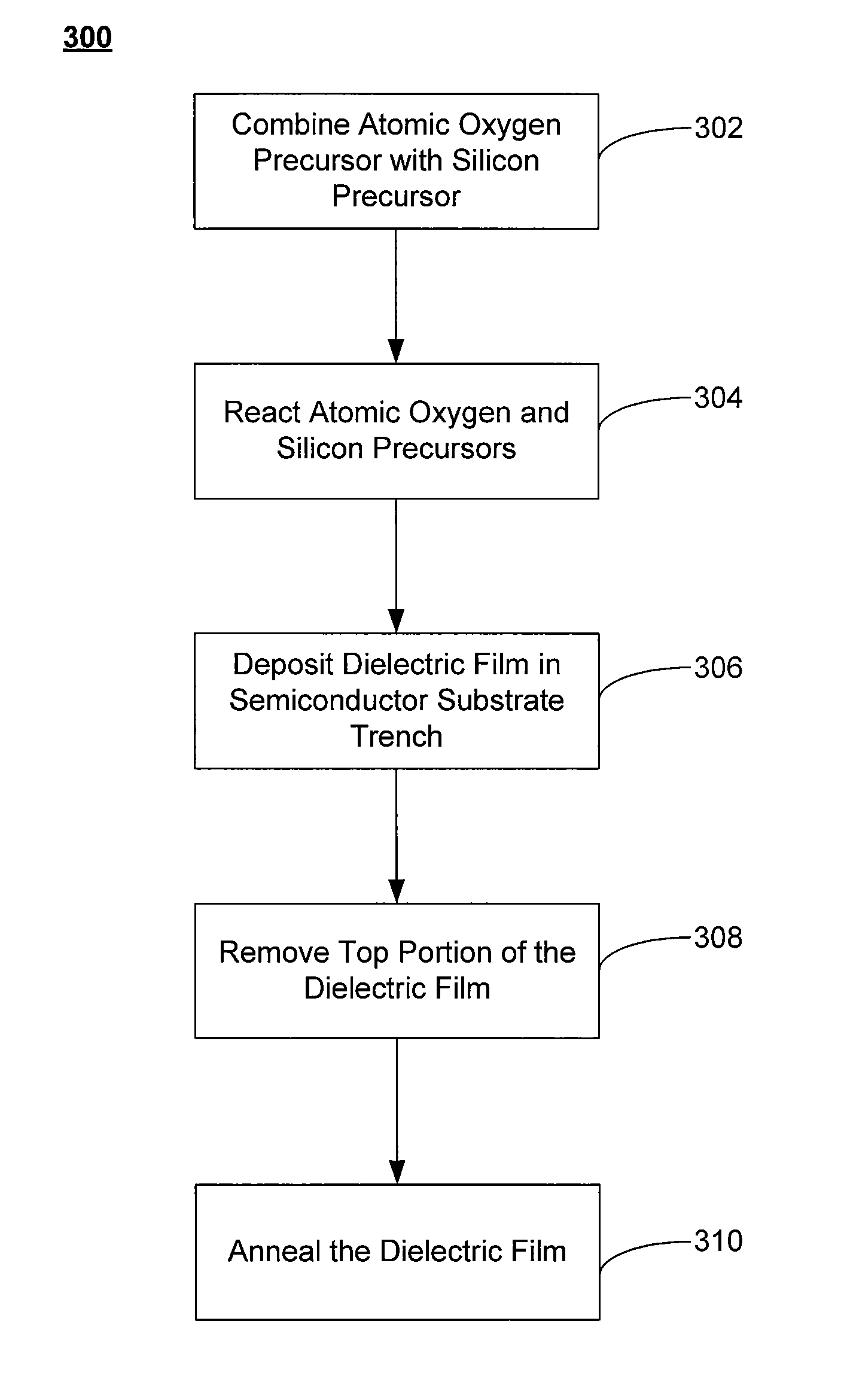
[0021]Embodiments of the invention include methods and systems for depositing dielectric materials in gaps and trenches within a surface of a substrate. The dielectric materials include silicon oxide films, which have wide application in the art, but the invention is not limited to any particular film composition, as will be evident from the description. Dielectric films deposited according to the techniques of the invention have excellent gapfill properties and can fill high-aspect-ratio gaps encountered in, for example, shallow trench isolation (STI) structures. Dielectric materials deposited by the methods and systems of the invention are particularly useful in filling gaps in 100-nm or smaller technology (e.g., 65 nm, 45 nm technology, etc.).

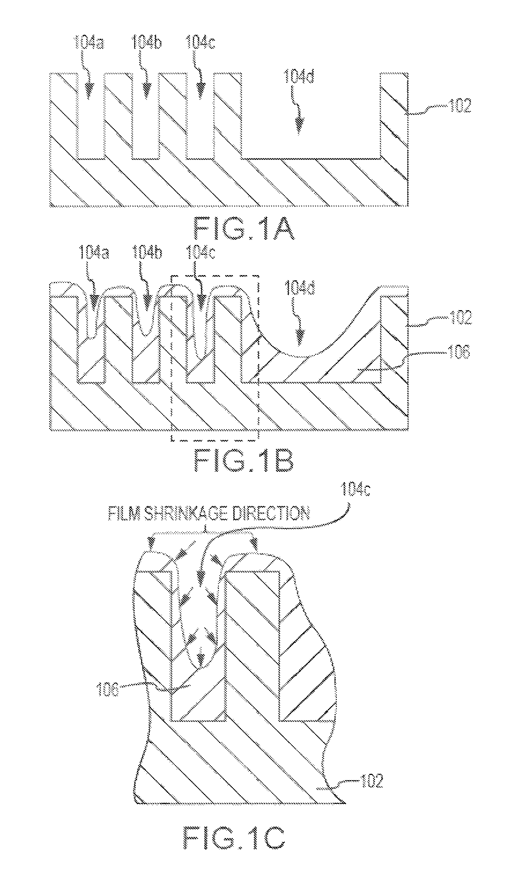
[0022]Dielectric depositions may include the formation of flowable dielectrics on the substrate that tend to collect in the bottom portion of a substrate gap or trench during the deposition. Because the flowable dielectric tends to migrate f...


PUM

PropertyMeasurementUnit
temperatureaaaaaaaaaa
internal pressureaaaaaaaaaa
temperatureaaaaaaaaaa

Abstract

Methods to reduce film cracking in a dielectric layer are described. The methods may include the steps of depositing a first dielectric film on a substrate and removing a top portion of the first dielectric film by performing an etch on the film. The methods may also include depositing a second dielectric film over the etched first film, and removing a top portion of the second dielectric film. In addition, the methods may include annealing the first and second dielectric films to form the dielectric layer, where the removal of the top portions from the first and the second dielectric films reduces a stress level in the dielectric layer.

Description

CROSS-REFERENCES TO RELATED APPLICATIONS[0001]This application claims the benefit of U.S. Provisional Application No. 60 / 805,573, filed Jun. 22, 2006, the entire contents of which are herein incorporated by reference for all purposes. This application is also related to U.S. patent application Ser. No. 11 / 753,918, filed May 25, 2007, and titled “A METHOD FOR DEPOSITING AND CURING LOW-K FILMS FOR GAPFILL AND CONFORMAL FILM APPLICATIONS”; and U.S. patent application Ser. No. 11 / 753,968, filed May 25, 2007,and titled “A NOVEL DEPOSITION-PLASMA CURE CYCLE PROCESS TO ENHANCE FILM QUALITY OF SILICON DIOXIDE”, of which the entire contents of both applications are herein incorporated by reference for all purposes.BACKGROUND OF THE INVENTION[0002]One of the persistent challenges faced in the development of semiconductor technology is the desire to increase the density of circuit elements and interconnections on substrates without introducing spurious interactions between them. Unwanted inter...

Claims


Application Information

Patent Timeline
Patent Type & Authority Patents(United States)
IPC IPC(8): H01L21/762
CPCH01L21/76229H01L21/76
Inventor LUBOMIRSKY, DMITRYNEMANI, SRINIVAS D.YIEH, ELLIE
Owner APPLIED MATERIALS INC
Why Eureka
Try Eureka