Method for manufacturing silicon carbide semiconductor device and the silicon carbide semiconductor device

a semiconductor device and semiconductor technology, applied in the direction of semiconductor devices, electrical appliances, basic electric elements, etc., can solve the problems of defective trench formation, high probability of semiconductor device breaking down, and prone to electrical field localization, so as to facilitate preventing the trenches prevent the deterioration or breakdown of silicon carbide semiconductor devices according to the invention, and facilitate the effect of preventing defects

Active Publication Date: 2012-07-31
FUJI ELECTRIC CO LTD
View PDF19 Cites 2 Cited by
  • Summary
  • Abstract
  • Description
  • Claims
  • Application Information

AI Technical Summary

Benefits of technology

[0048]According to the invention, the trench sections connecting the end portions of the first straight trenches are connected to form a polygon, depending on the spacing between the first straight trenches (cell pitch), having side walls which are hardly deformed by a heat treatment (such as half the circumference of a hexagon, half the circumference of a dodecagon, half the circumference of an octadecagon and half the circumference of a triacontagon). Therefore, it is possible to manufacture a silicon carbide semiconductor device that facilitates preventing the trenches thereof from being filled by the heat treatment conducted at 1500° C. or higher. Since it is possible to manufacture a silicon carbide semiconductor device that includes no end portions left in the trench according to the invention, the electric field is prevented from localizing to the end portions of the trench. Therefore, it is possible to prevent the silicon carbide semiconductor device according to the invention from being deteriorated or broken down.
[0049]The manufacturing methods according to the invention facilitate preventing defects from causing in the silicon carbide semiconductor devices.

Problems solved by technology

When a pointing trench end portion is caused by dry etching, electric field localization is liable to be caused at the pointing trench end portion.
As the electric field localizes to the trench end portion and exceeds the breakdown voltage of the semiconductor device to the higher side, there is a high probability that the semiconductor device will break down.
If a part of the connecting trench section is deformed greatly by the unevenness caused by the heat treatment, the unevenness itself will cause defective trench formation.
If the electric field localizes to the trench end portion, the SiC semiconductor device will be deteriorated or broken down.

Method used


Image

  • Method for manufacturing silicon carbide semiconductor device and the silicon carbide semiconductor device
  • Method for manufacturing silicon carbide semiconductor device and the silicon carbide semiconductor device
  • Method for manufacturing silicon carbide semiconductor device and the silicon carbide semiconductor device

Examples


first embodiment

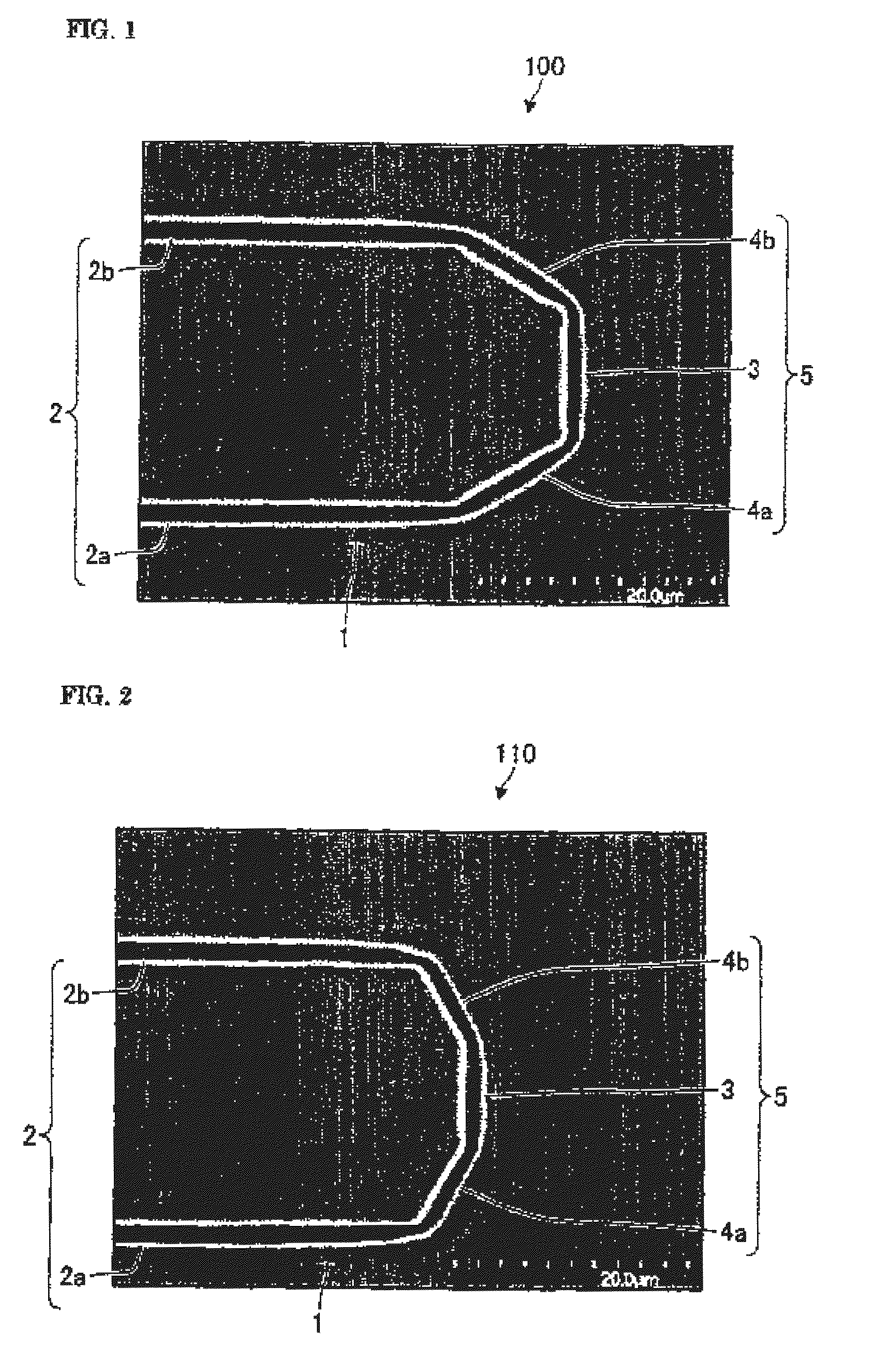
[0097]FIG. 1 is an electron micrograph that observes the surface of a silicon carbide semiconductor device according to a first embodiment of the invention.

[0098]Silicon carbide semiconductor device (hereinafter referred to as “SiC semiconductor device”) 100 includes, for example, an SiC single crystal substrate or a substrate including an SiC single crystal substrate and an SiC epitaxial layer on the SiC single crystal substrate (hereinafter referred to collectively as an “SiC substrate”) and trench 1 formed in the surface portion of the SiC substrate. Trench 1 is formed of adjoining straight trenches (hereinafter referred to as “straight trench section”) 2 and connecting trench section 5 connecting the end portions of straight trench section 2. In the SiC substrate, a plurality of trenches 1 is disposed almost in parallel to straight trench section 2, for example, in a stripe pattern. Straight trench section 2 corresponds to a first trench section.

[0099]Straight trench section 2 i...

second embodiment

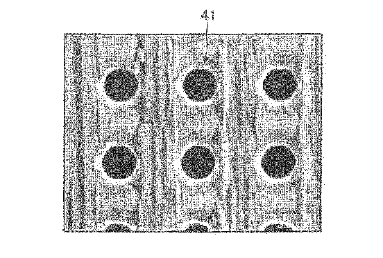
[0125]FIG. 6 is an electron micrograph that observes the surface of a silicon carbide semiconductor device according to a second embodiment of the invention. FIG. 7 is an electron micrograph that observes the surface of the silicon carbide semiconductor device shown in FIG. 6 before the heat treatment thereof.

[0126]The SiC semiconductor device according to the second embodiment may be obtained by adding fourth and fifth connecting trenches to connecting trench section 5 of the SiC semiconductor device according to the first embodiment.

[0127]In SiC semiconductor device 140 according to the second embodiment, second connecting trench 4a connects the end portion of first straight trench 2a and the first end portion of fourth connecting trench 7a. The second end portion of fourth connecting trench 7a is connected to the first end portion of first connecting trench 3. Third connecting trench 4b connects the end portion of second straight trench 2b and the first end portion of fifth conne...

third embodiment

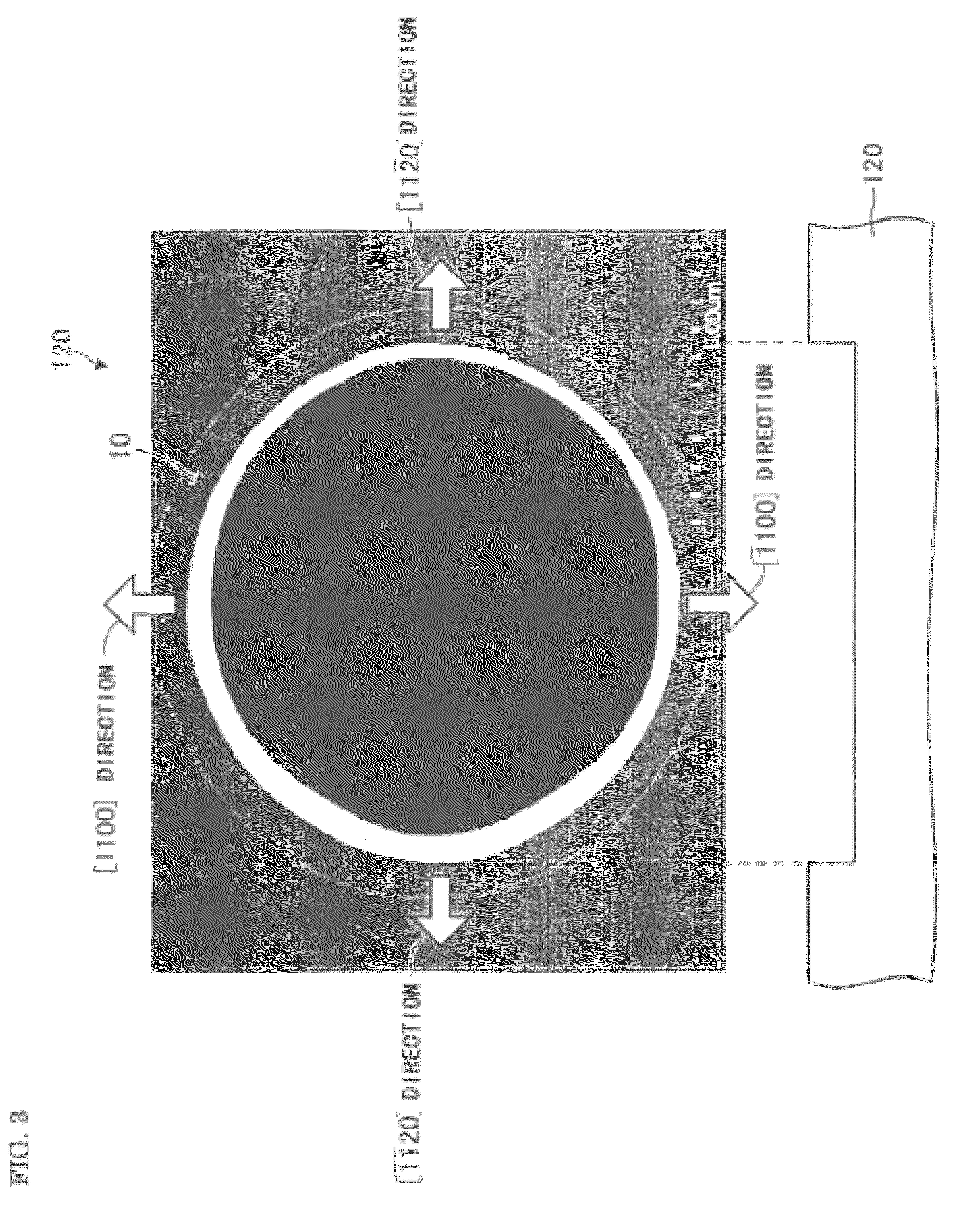
[0131]FIG. 8 is an electron micrograph that observes the surface of a silicon carbide semiconductor device according to a third embodiment of the invention. FIG. 9 is an electron micrograph that observes the surface of the silicon carbide semiconductor device shown in FIG. 8 before the heat treatment thereof.

[0132]The manufacturing method for manufacturing SiC semiconductor device 150 and the conditions under which trenches are formed are the same as those for SiC semiconductor device 100 according to the first embodiment. It is effective to dispose a vertical and straight connecting trench extending vertically to straight trench section 2 (hereinafter referred to as a “vertical straight connecting trench”) in substitution for connecting trench section 5 in the SiC semiconductor device 100 according to the first embodiment. The end portion formed inside trench 1 by straight trench section 2 and the vertical straight connecting trench is set to be polygonal. The widths of the end por...


PUM


Abstract

Silicon carbide semiconductor device includes trench, in which connecting trench section is connected to straight trench section. Straight trench section includes first straight trench and second straight trench extending in parallel to each other. Connecting trench section includes first connecting trench perpendicular to straight trench section, second connecting trench that connects first straight trench and first connecting trench to each other, and third connecting trench that connects second straight trench and first connecting trench to each other. Second connecting trench extends at 30 degrees of angle with the extension of first straight trench. Third connecting trench extends at 30 degrees of angle with the extension of second straight trench. A manufacturing method according to the invention for manufacturing a silicon carbide semiconductor device facilitates preventing defects from being causes in a silicon carbide semiconductor device during the manufacture thereof.

Description

BACKGROUND OF THE INVENTION[0001]A. Field of the Invention[0002]The present invention relates to a method for manufacturing a silicon carbide semiconductor device and the silicon carbide semiconductor device. Specifically, the invention relates to a method for manufacturing a silicon carbide semiconductor device having a trench structure and the silicon carbide semiconductor device having a trench structure.[0003]B. Description of the Related Art[0004]In the semiconductor devices such as a metal oxide semiconductor field effect transistor (hereinafter referred to as a “MOSFET”) and an insulated gate bipolar transistor (hereinafter referred to as an “IGBT”) having a trench structure, straight trenches, for example, are formed in a stripe pattern from the surface of a semiconductor substrate.[0005]In the semiconductor devices having a straight trench structure, electric field localization occurs at the end portion of the trench, when a high voltage is applied to the semiconductor devi...

Claims


Application Information

Patent Timeline
Patent Type & Authority Patents(United States)
IPC IPC(8): H01L21/02
CPCH01L21/0475H01L29/7827H01L29/66068H01L29/045H01L29/1608H01L21/302H01L21/3065H01L21/3081H01L21/31116H01L21/31138H01L29/7397H01L29/4238H01L29/7813
Inventor KAWADA, YASUYUKITAWARA, TAKESHI
Owner FUJI ELECTRIC CO LTD
Why Eureka
Try Eureka