Output stage for a digital RF transmitter, method for providing an RF output signal in a digital RF transmitter, and digital RF transmitter

a digital rf transmitter and output stage technology, applied in the direction of amplifiers, electrical apparatus, semiconductor devices/discharge tubes, etc., can solve the problems of shortening the battery life, low power efficiency of linear power amplifiers compared to non-linear power amplifiers, and reducing the size of sections, so as to improve overall power efficiency and reduce the size of sections

Inactive Publication Date: 2012-08-07
AMPLEON NETHERLANDS
View PDF6 Cites 5 Cited by
  • Summary
  • Abstract
  • Description
  • Claims
  • Application Information

AI Technical Summary

Benefits of technology

[0011]It is an object of the present invention to provide an output stage for a digital RF transmitter, a method for providing an RF output signal in a digital RF transmitter, and a digital RF transmitter with which input interpolation is possible with reduced size of sections of the output stage and with which the maximum operating frequency can be enhanced. Further, the overall power efficiency shall be improved.
[0012]This object is attained by an output stage for a digital RF transmitter according to claim 1. The output stage comprises: an input adapted to receive an input signal to be transmitted; a plurality N of power amplification sections; and an output providing an output voltage signal. Each of the N power amplification sections is arranged to receive the input signal and comprises a transformer adapted to provide a respective output signal, each transformer comprising a primary stage and a secondary stage. The secondary stages of the transformers of the N power amplification sections are combined such that a combined output voltage signal of the output stage is provided. The N power amplification sections are adapted such that the input signal is latched by clock signals comprising different phases. In this context, the term input signal covers both unary and binary RF envelope data. Since each of the N power amplification sections comprises a transformer providing the respective output voltage signal, instead of summing output currents employed in conventional approaches, the output voltage can be stacked. In each power amplification section, the size of the unit array can be much smaller than the transformer size. As a result, the maximum operating frequency is enhanced. Since the input signal is latched by clock signals comprising different phases in the N power amplification sections, the output voltage swing is evenly distributed in N sections, resulting in a lower voltage swing in each section. Therefore, it is possible to use thin oxide transistors to achieve high power efficiency at high output power such that the need for an external power amplifier is eliminated.
[0013]Preferably, the N power amplification sections are arranged such that interpolation of the input signal is provided. Thus, introduced spectral image can be suppressed conveniently.
[0015]According to an aspect, at least one of the N power amplification sections is provided with a switch structure capable of switching the respective output signal of that section on and off. As a result, the power efficiency of the output stage can be improved, since the amplifier can be controlled to operate at peak efficiency over a large power range by turning on / off each section.
[0017]The object is further attained by a method for providing an RF output signal in a digital RF transmitter according to claim 6. The method comprises the steps: applying an input signal at a plurality N of power amplification sections of an output stage; latching the input signal by clock signals comprising different phases in the plurality N of power amplification sections; applying respective RF output signals of the plurality N of power amplification sections to corresponding transformers, and combining secondary stages of the transformers of the N power amplification sections such that a combined output voltage signal of the output stage is provided. Since the RF output signals of the N power amplification sections are each provided to a transformer, instead of summing output currents employed in conventional approaches, the output voltage can be stacked. In each power amplification section, the size of the unit array can be much smaller than the transformer size, thus enhancing the maximum operating frequency. Since the input signal is latched by clock signals comprising different phases in N power amplification sections, the output voltage swing is evenly distributed in N sections, resulting in a lower voltage swing in each section. Therefore, it is possible to use thin oxide transistors to achieve high power efficiency at high output power such that the need for an external power amplifier is eliminated.
[0019]Preferably, at least one of the plurality of power amplification sections is switched on and off depending on the output power level. In this case, the average power efficiency is improved, since the amplifier can operate at peak efficiency over a large power range.

Problems solved by technology

However, the power efficiency of linear power amplifiers is still low as compared to non-linear power amplifiers.
Thus, in mobile applications this shortens the battery life.
However, the efficiency of these techniques remains limited due to the use of linear power amplifiers.
However, with such a technique as well, problems occur which will be described in the following.
However, in practice the bandwidth of the DC-DC converter in the amplitude path is limited.
Further, in the amplitude modulation path, spectrum re-growth occurs which leads to a much larger bandwidth than that of the desired RF output signal.
Due to this, such an arrangement using the DC-DC converter is only suitable to standards for data transmission with a very narrow bandwidth, such as GSM and EDGE standards.
However, this leads to a reduction in power efficiency.
However, in real implementation a problem occurs that the binary weighted array cannot guarantee a monotonic output current.
This is due to an inevitable mismatch of the employed transistors.
This may violate the spectral mask and the constraints with respect to out-of-band emissions.
However, filtering the output requires an extra LC tank and frequency tuning.
Thus, for on-chip integration this is disadvantageous because it results in large chip area and complex circuitry.
However, in this approach similar problems with respect to the image spectrum occur as in the direct envelope modulator.
As a consequence, the operating frequency is limited.

Method used


Image

  • Output stage for a digital RF transmitter, method for providing an RF output signal in a digital RF transmitter, and digital RF transmitter
  • Output stage for a digital RF transmitter, method for providing an RF output signal in a digital RF transmitter, and digital RF transmitter
  • Output stage for a digital RF transmitter, method for providing an RF output signal in a digital RF transmitter, and digital RF transmitter

Examples


Embodiment Construction

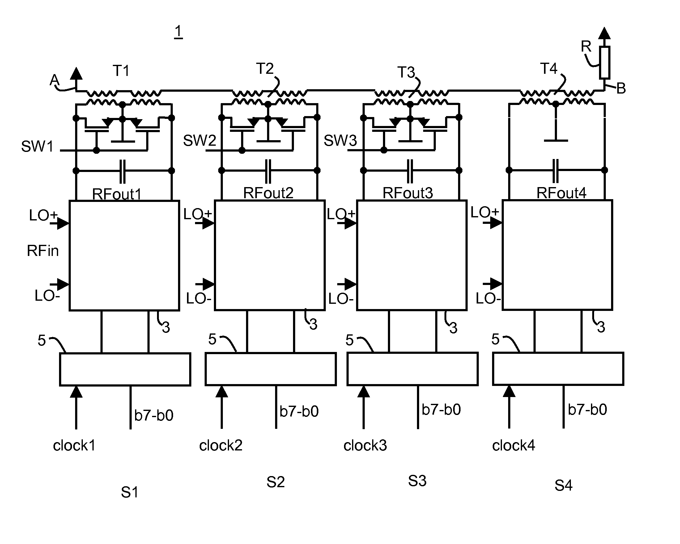
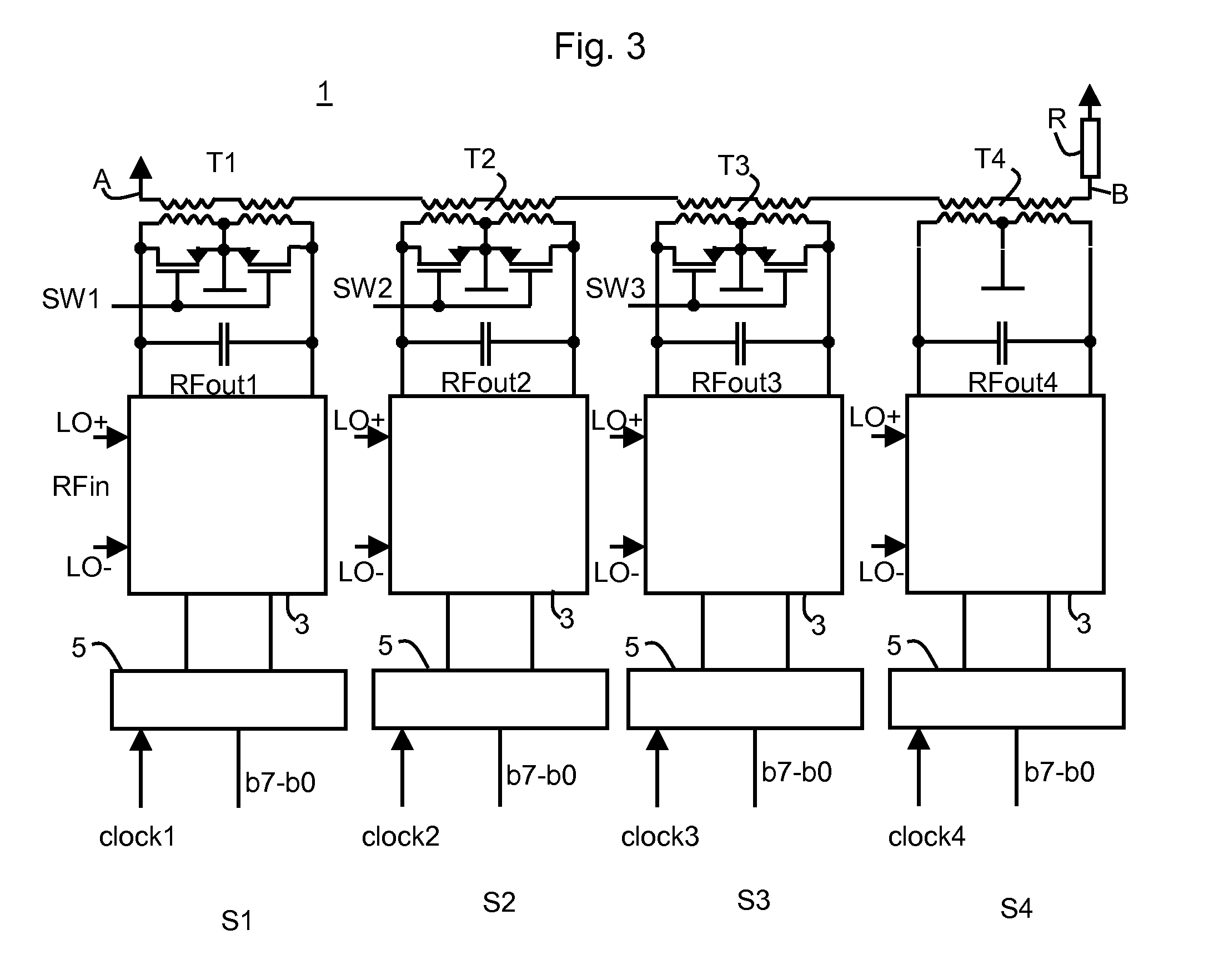
[0028]An embodiment of the invention will now be described with respect to FIGS. 3 to 5. According to the embodiment, the output stage 1 comprises four power amplification sections S1, S2, S3, and S4 (i.e. N=4 in the present embodiment). It should be noted that the invention is not limited to N=4 and other numbers are possible as well. However, N>2 is preferred and N>3 is more preferred. Each of the power amplification sections S1, S2, S3, and S4 is formed by a thermometer-coded envelope-modulated polar amplifier. In the following, the functioning of this thermometer-coded envelope-modulated polar amplifier will be described with reference to FIGS. 4 and 5 for the power amplification section S1.

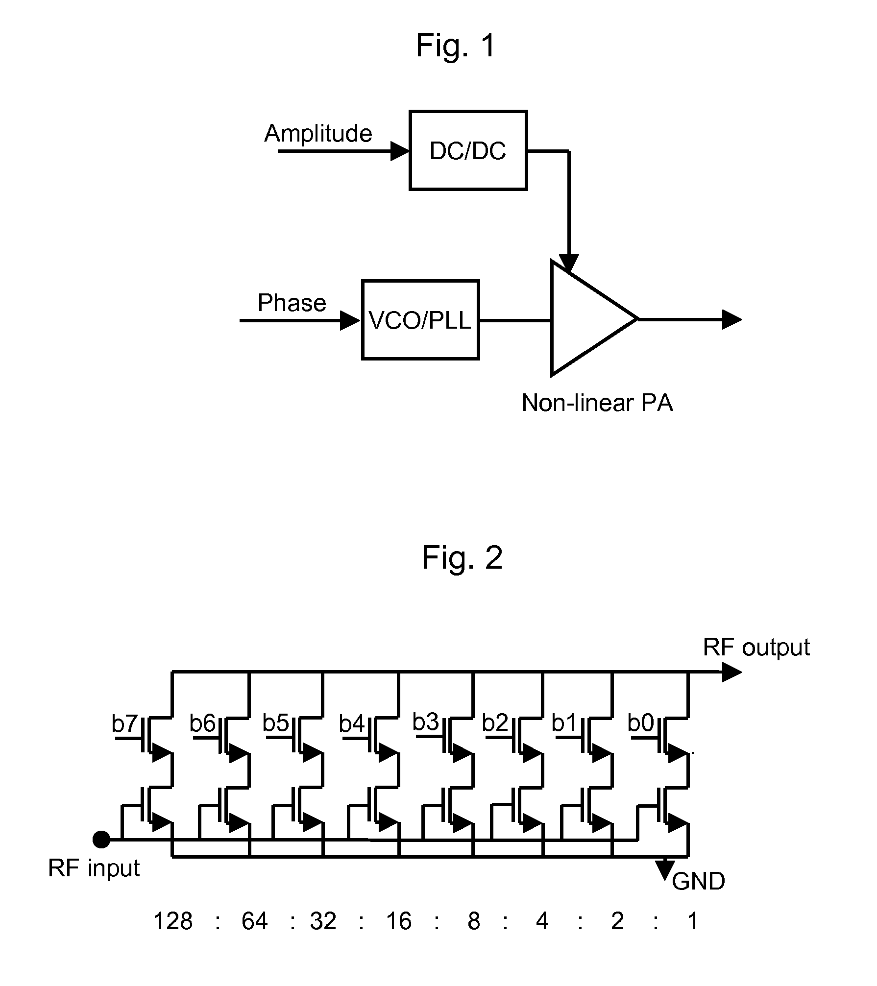
[0029]As shown in FIGS. 4 and 5, the thermometer-coded envelope-modulated polar amplifier 2 comprises a unit array 3 which in the present embodiment has 256 (16×16) unit cells 4 arranged in 16 rows and 16 columns. Thus, the polar amplifier 2 is adapted for 8-bit data. A skilled person will un...


PUM


Abstract

An output stage (1) for a digital RF transmitter is provided. The output stage comprises: an input adapted to receive an input signal (RFin, b7-b0) to be transmitted; a plurality N of power amplification sections (S1, S2, S3, S4); and an output (A, B) providing an output voltage signal. Each of the N power amplification sections (S1, S2, S3, S4) is arranged to receive the input signal (RFin, b7-b0) and comprises a transformer (T1, T2, T3, T4) adapted to provide a respective output signal. Each transformer comprises a primary stage and a secondary stage; the secondary stages of the transformers (T1, T2, T3, T4) of the N power amplification sections (S1, S2, S3, S4) are combined such that a combined output voltage signal of the output stage is provided. The N power amplification sections (S1, S2, S3, S4) are adapted such that the input signal (RFin, b7-b0) is latched by clock signals (clock1, clock2, clock3, clock4) comprising different phases.

Description

FIELD OF THE INVENTION[0001]The invention relates to an output stage for a digital RF transmitter, to a method for providing an RF output signal in a digital RF transmitter, and to a digital RF transmitter. More general, the present invention relates to the field of wireless data conversion. More specifically, it relates to the field of digital RF transmitters, which can e.g. be used for transmitting data in wireless communication systems.BACKGROUND OF THE INVENTION[0002]In recent years, an increased demand for higher data-rate wireless communications has arisen. This demand has led to the widespread adoption of non-constant envelope modulation which presents higher spectrum efficiency for data transmission. Conventional systems applying non-constant envelope modulation require use of linear power amplifiers (PAs). However, the power efficiency of linear power amplifiers is still low as compared to non-linear power amplifiers. Thus, in mobile applications this shortens the battery l...

Claims


Application Information

Patent Timeline
Patent Type & Authority Patents(United States)
IPC IPC(8): H03F3/26
CPCH04B1/0483
Inventor HE, XINCOLLADOS ASENSIO, MANELPAVLOVIC, NENADVAN SINDEREN, JAN
Owner AMPLEON NETHERLANDS
Why Eureka
Try Eureka