Inertial sensor
a sensor and inner tube technology, applied in the field ofinertial sensors, can solve the problems of not being able to vibrate the vibrating body in a state with high frequency and large amplitude, and the fine vibrating body formed by micromachining techniques is greatly affected, so as to improve the detection sensitivity of the angular rate sensor, suppress the displacement sensitive, and improve the detection sensitivity of the acceleration sensor
- Summary
- Abstract
- Description
- Claims
- Application Information
AI Technical Summary
Benefits of technology
Problems solved by technology
Method used
Image
Examples
first embodiment
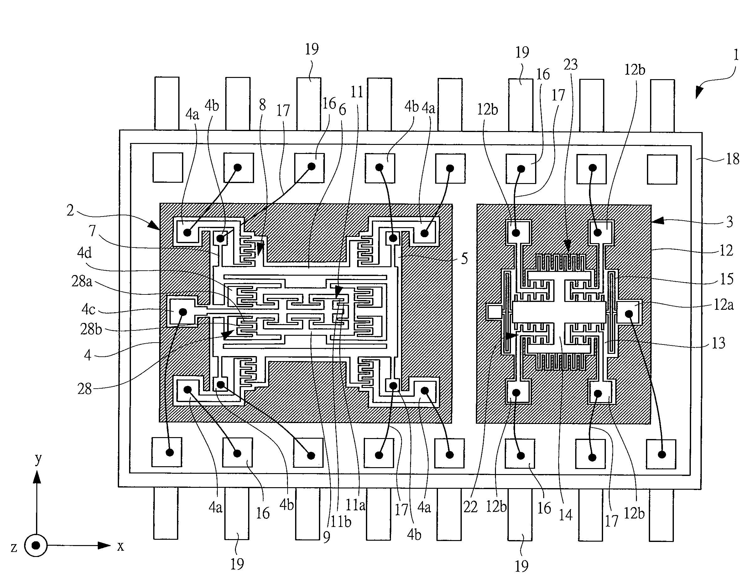
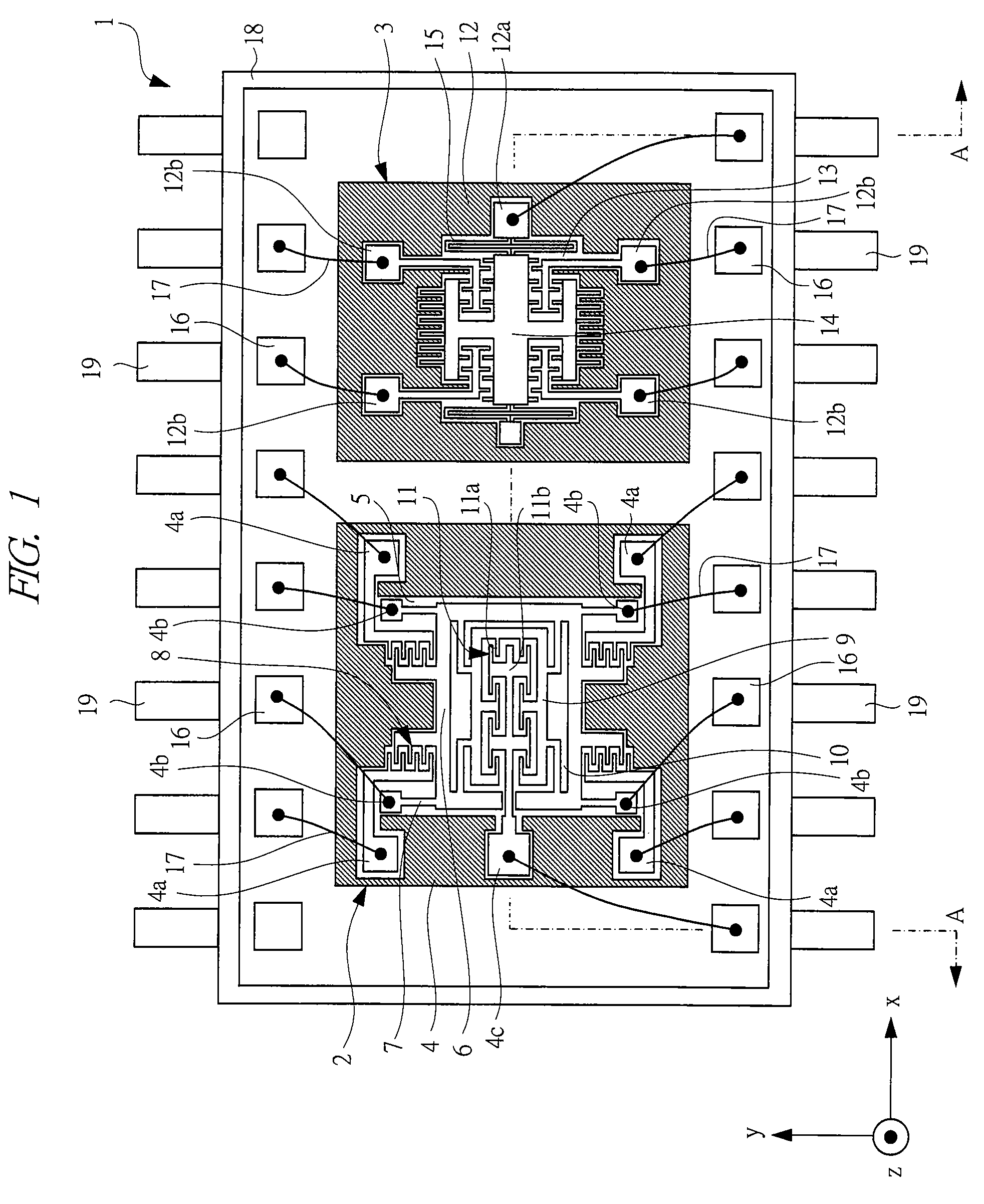
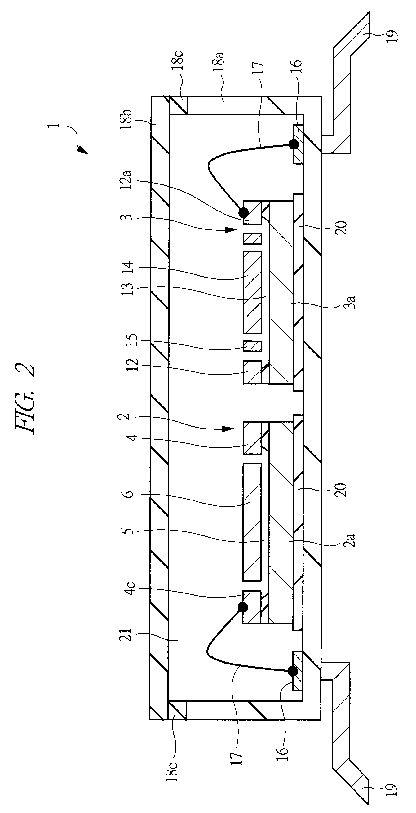
[0036]An inertial sensor in a first embodiment will be described with reference to the drawings. FIG. 1 is a plan view showing an inertial sensor according to the first embodiment. In FIG. 1, an inertial sensor 1 includes an angular rate sensor 2 and an acceleration sensor 3. In FIG. 1, the angular rate sensor 2 and the acceleration sensor 3 are formed in separate semiconductor chips.
[0037]First, a configuration of the angular rate sensor 2 will be described. As shown in FIG. 1, the angular rate sensor 2 has a cavity portion (first cavity portion) 5 formed in the interior of a rectangular periphery portion (first periphery portion) 4. In the interior of this cavity portion 5, a fixing portion 4a, a fixing portion (first fixing portion) 4b, a fixing portion 4c, and a vibrating body 6 are formed. The vibrating body 6 is connected to the fixing portion 4b by an elastic deforming portion (first elastic deforming portion; support beam) 7. Further, between this vibrating body 6 and the fi...
second embodiment
[0077]While descriptions have been made on the example in which the angular rate sensor and the acceleration sensor are formed in separate semiconductor substrates (semiconductor chips) in the first embodiment, in the second embodiment, descriptions will be made on an example in which the angular rate sensor and the acceleration sensor are formed in the same semiconductor substrate (semiconductor chip).
[0078]FIG. 5 is a plan view showing an inertial sensor 1 in the second embodiment. As shown in FIG. 5, the packaging method of the inertial sensor 1, the internal gas pressure, the configuration and the effect of the shift suppressing portion (damper) 23 are the same as the already described case where the acceleration sensor and the angular rate sensor are formed on the separate semiconductor substrates. A difference lies in the point that the angular rate sensor and the acceleration sensor are formed on the same semiconductor substrate. That is, since the angular rate sensor and the...
third embodiment
[0082]For example, in an inertial sensor in which an acceleration sensor and an angular rate sensor are integrated on the same semiconductor substrate (one chip), the acceleration sensor and the angular rate sensor can be disposed inside a space of the same kind and having the same pressure. Hence, the inertial sensor can be managed easily by a wafer level package (WLP) as shown in FIG. 7. While the angular rate sensor and the acceleration sensor are formed in the individual chip areas formed in the semiconductor wafer, before singulating the chip area formed with the angular rate sensor and the acceleration sensor, a technique for sealing each chip area by a cap is referred to as a wafer level package. FIG. 7 is a schematic cross-sectional view showing a configuration of the inertial sensor subjected to wafer level packaging, and showing a state in which the angular rate sensor and the acceleration sensor formed on the same semiconductor substrate 25a are sealed by a cap 27, and th...
PUM
 Abstract
Description
Claims
Application Information


