Power semiconductor devices and methods for manufacturing the same

a technology of power semiconductors and semiconductor devices, applied in the field of semiconductor devices, can solve the problems of difficult to form only a region, and limited n-type region of heavily doped region, so as to improve the relevant tradeoff characteristics, reduce cracks and partings in the wafer, and prevent expansion

Inactive Publication Date: 2012-09-04
FUJI ELECTRIC CO LTD
View PDF18 Cites 4 Cited by
  • Summary
  • Abstract
  • Description
  • Claims
  • Application Information

AI Technical Summary

Benefits of technology

[0040]The steps, performed after the semiconductor substrate is thinned, are decreased as compared with the conventional manufacturing method for manufacturing a semiconductor substrate. Therefore, the cracks and partings caused in the wafer are reduced. By providing the semiconductor substrate of the first conductivity type with an impurity concentration distribution in parallel to the major surface thereof, a space charge region is prevented from expanding at the time of turnoff by the lightly doped semiconductor layer. The extremely lightly doped semiconductor layer expands the space charge region to eject the electrons and holes quickly. Therefore, the relevant tradeoff characteristics are improved and the soft switching performances are obtained at the same time.
[0041]By the semiconductor devices and method for manufacturing the semiconductor devices according to the invention, the relevant tradeoff characteristics are improved and the soft switching performances are obtained at the same time. By the manufacturing method according to the invention, the manufacturing steps for manufacturing a semiconductor device are reduced and a semiconductor substrate that provides more degrees of freedom for designing a semiconductor device is manufactured.

Problems solved by technology

The ON-state-voltage turnoff-power-loss tradeoff characteristics and the soft switching performances are not simultaneously improved very often by the conventional methods known to persons skilled in the art.
Therefore, it has been an important problem to improve both the ON-state-voltage turnoff-power-loss tradeoff characteristics and the soft switching performances at the same time.
It is difficult to form only a region doped more heavily than the semiconductor substrate, in the semiconductor substrate.
Moreover, the heavily doped region is limited to an n-type region.
Therefore, a soft switching performance is not obtained.

Method used


Image

  • Power semiconductor devices and methods for manufacturing the same
  • Power semiconductor devices and methods for manufacturing the same
  • Power semiconductor devices and methods for manufacturing the same

Examples


embodiments

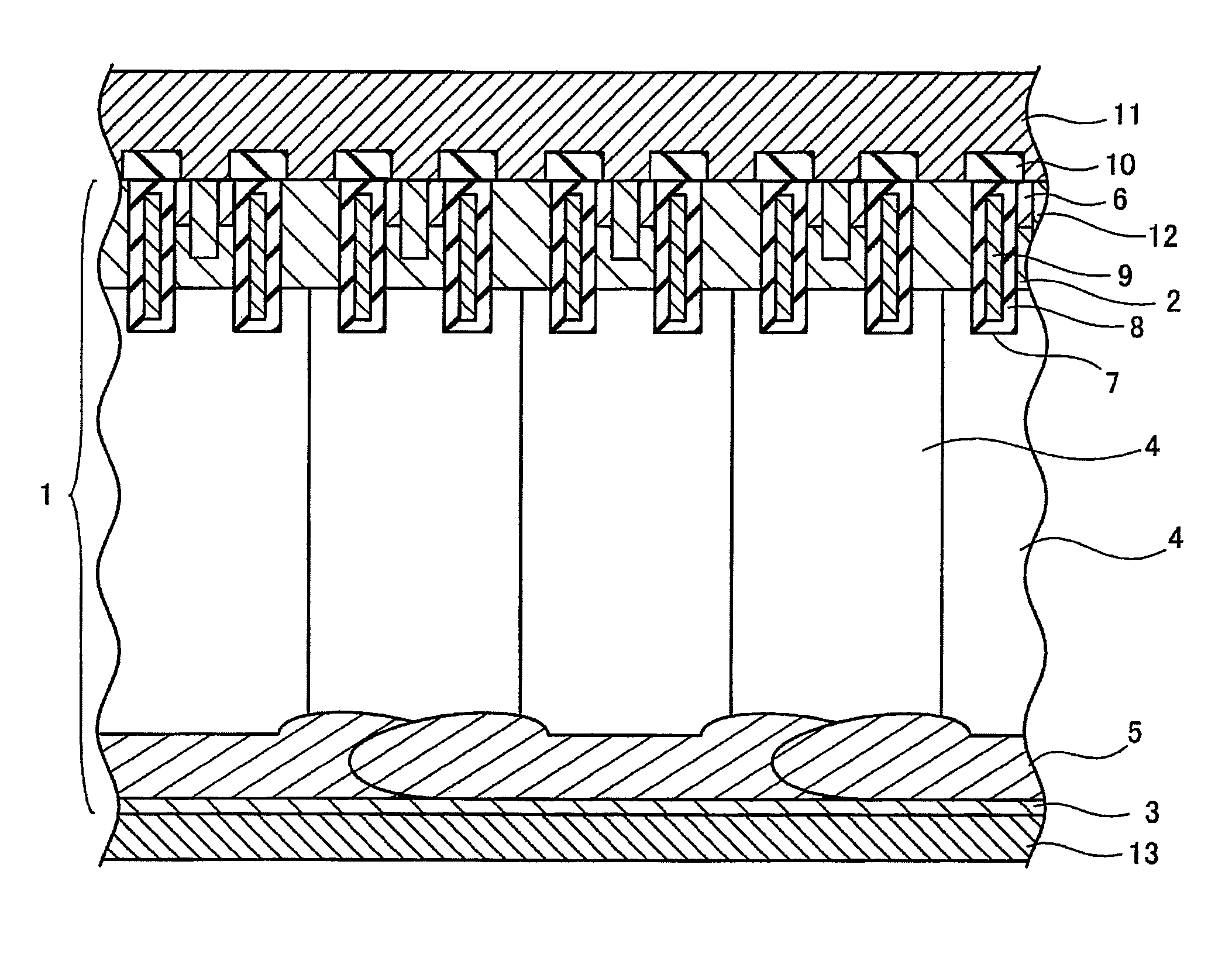
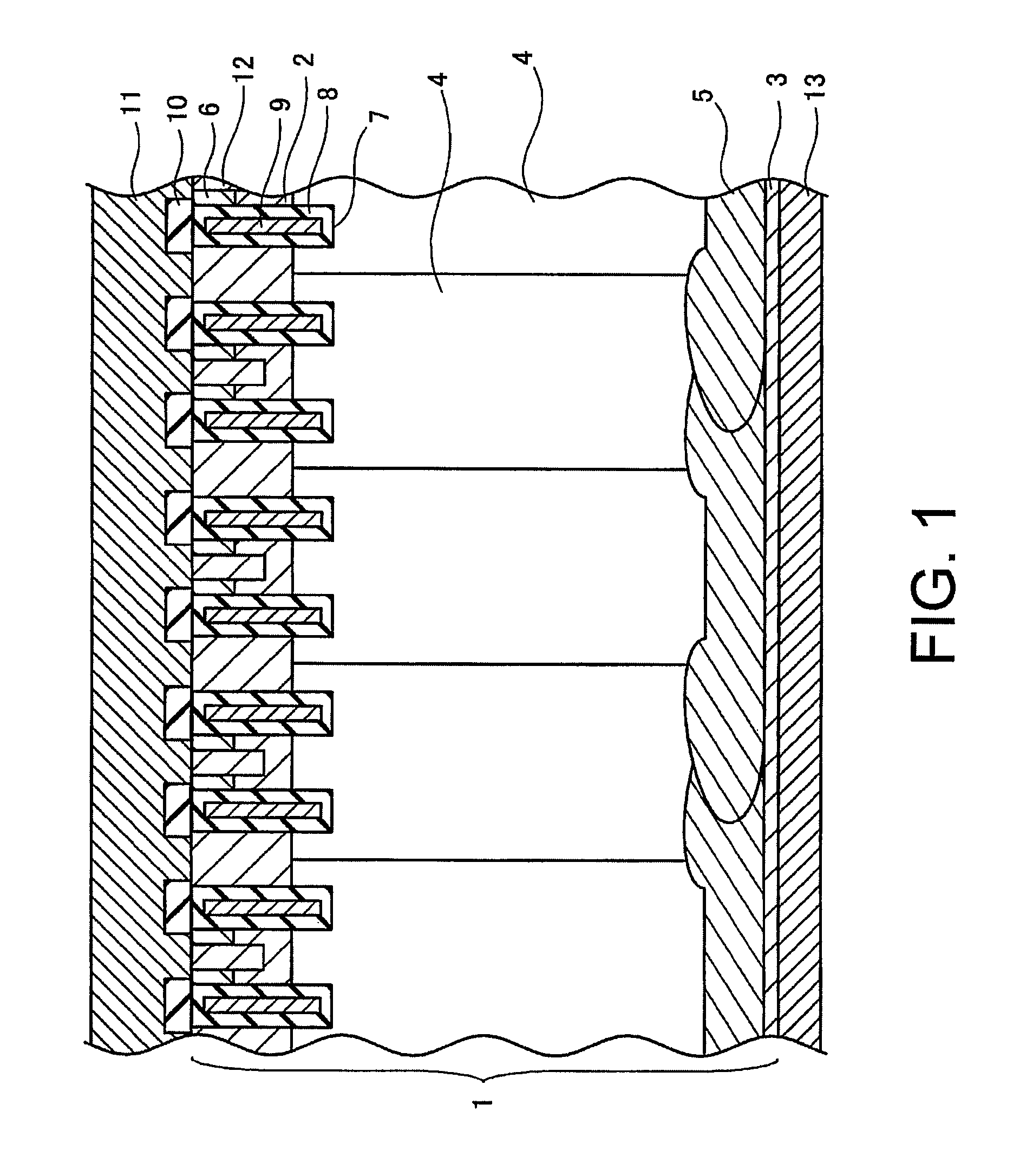
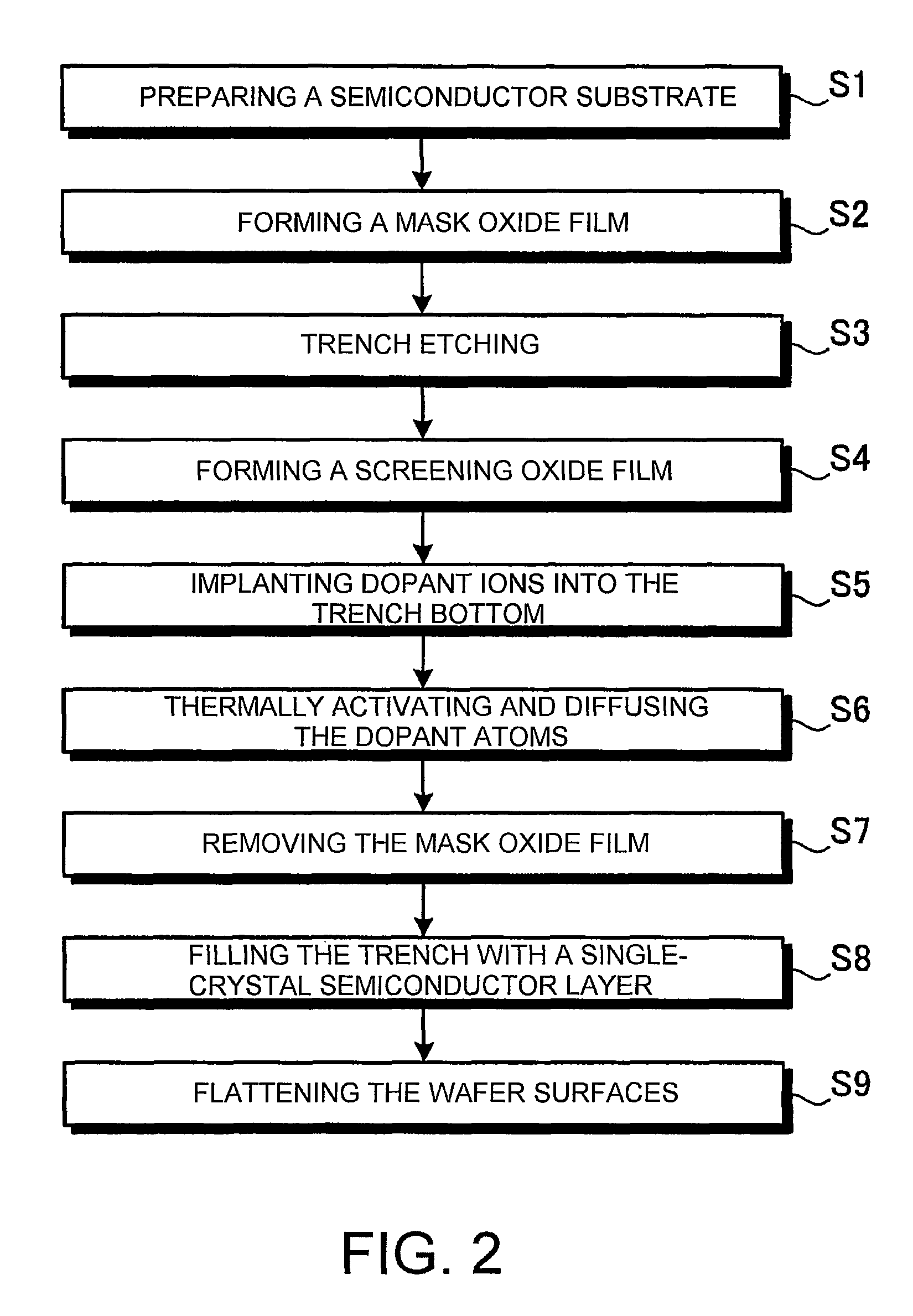
[0162]A PIN diode is manufactured by the manufacturing method according to the fifth mode for carrying out the invention. An n-type floating-zone silicon substrate cut out from a silicon ingot prepared by the floating zone method (hereinafter referred to as the “FZ method”) is used as a starting substrate. (Hereinafter the floating-zone silicon substrate will be referred to as the “FZ silicon substrate”.) The resistivity of the FZ silicon substrate is 40Ω·cm. The thickness of the FZ silicon substrate is 500 μm. The orientation of the plane of the FZ silicon substrate is (100). The direction of orientation flat of the FZ silicon substrate is .

[0163]A mask oxide film of 2.4 μm in thickness is formed, for example, by a thermal oxidation treatment on the first major surface of the FZ silicon substrate. Then, the mask oxide film is removed by photolithographic and etching techniques for a width of 10 μm and with spaces of 10 μm to expose the first major surface of the FZ silicon substrat...


PUM


Abstract

A power semiconductor device that realizes high-speed turnoff and soft switching at the same time has an n-type main semiconductor layer that includes lightly doped n-type semiconductor layers and extremely lightly doped n-type semiconductor layers arranged alternately and repeatedly between a p-type channel layer and an n+-type field stop layer, in a direction parallel to the first major surface of the n-type main semiconductor layer. A substrate used for manufacturing the semiconductor device is fabricated by forming trenches in an n-type main semiconductor layer 1 and performing ion implantation and subsequent heat treatment to form an n+-type field stop layer in the bottom of the trenches. The trenches are then filled with a semiconductor doped more lightly than the n-type main semiconductor layer for forming extremely lightly doped n-type semiconductor layers. The manufacturing method is applicable with variations to various power semiconductor devices such as IGBT's, MOSFET's and PIN diodes.

Description

FIELD OF THE INVENTION[0001]The present invention relates to semiconductor devices and methods for manufacturing the semiconductor devices. Specifically, the invention relates to semiconductor devices such as insulated gate bipolar transistors (hereinafter referred to as “IGBT's”), metal oxide semiconductor field effect transistors (hereinafter referred to as “MOSFET's”) and PIN diodes that constitute power semiconductor devices. The invention relates also to the methods for manufacturing these power semiconductor devices.BACKGROUND OF THE INVENTION[0002]Generally, power semiconductor devices have been used as non-contact switches. Therefore, it has been required for the power semiconductor devices to produce lower losses therein. For reducing the losses produced therein, techniques for ON-state voltage lowering and switching loss reduction have been explored. It has been known to persons skilled in the art that there exists a tradeoff relationship between the ON-state voltage and t...

Claims


Application Information

Patent Timeline
Patent Type & Authority Patents(United States)
IPC IPC(8): H01L21/336
CPCH01L29/0634H01L29/0878H01L29/66348H01L29/868H01L29/7397H01L29/7802H01L29/66712
Inventor YOSHIKAWA, KOH
Owner FUJI ELECTRIC CO LTD
Why Eureka
Try Eureka