Convex shaped thin-film transistor device

a thin-film transistor and convex technology, applied in semiconductor devices, semiconductor/solid-state device details, radiation controlled devices, etc., can solve the problems of limiting the amount of storage capacity and density of each memory cell, and difficulty in so as to achieve easy higher storage capacity and density, the effect of shortening the distance between the bit lines

Active Publication Date: 2012-09-11
MONTEREY RES LLC
View PDF8 Cites 26 Cited by
  • Summary
  • Abstract
  • Description
  • Claims
  • Application Information

AI Technical Summary

Benefits of technology

[0006]The present invention has been made in view of the above circumstances and provides a semiconductor device and a method of manufacturing the semiconductor device by which the distance between bit lines can be shortened and higher storage capacity and density can be achieved.
[0007]According to an aspect of the present invention, there is provided a semiconductor device including: first bit lines that are provided on a substrate; an insulating layer that is provided between the first bit lines on the substrate, and has a higher upper face than the first bit lines; channel layers that are provided on both side faces of the insulating layer, and are coupled to the respective first bit lines; and charge storage layers that are provided on opposite side faces of the channel layers from the side faces on which the insulating layers are formed At least part of the channel layers is formed in a different direction from the direction of the surface of the substrate. Accordingly, the channel length can be made larger. Thus, a semiconductor device that has a shorter distance between the bit lines and can easily achieve higher storage capacity and density can be provided.

Problems solved by technology

Also, a substrate current flows between the bit lines on the substrate side, which is called “punchthrough.” Therefore, it is difficult to shorten the distance between the bit lines, and there is a limit to the amount the storage capacity and density of each memory cell can be increased.

Method used


Image

  • Convex shaped thin-film transistor device
  • Convex shaped thin-film transistor device
  • Convex shaped thin-film transistor device

Examples


first embodiment

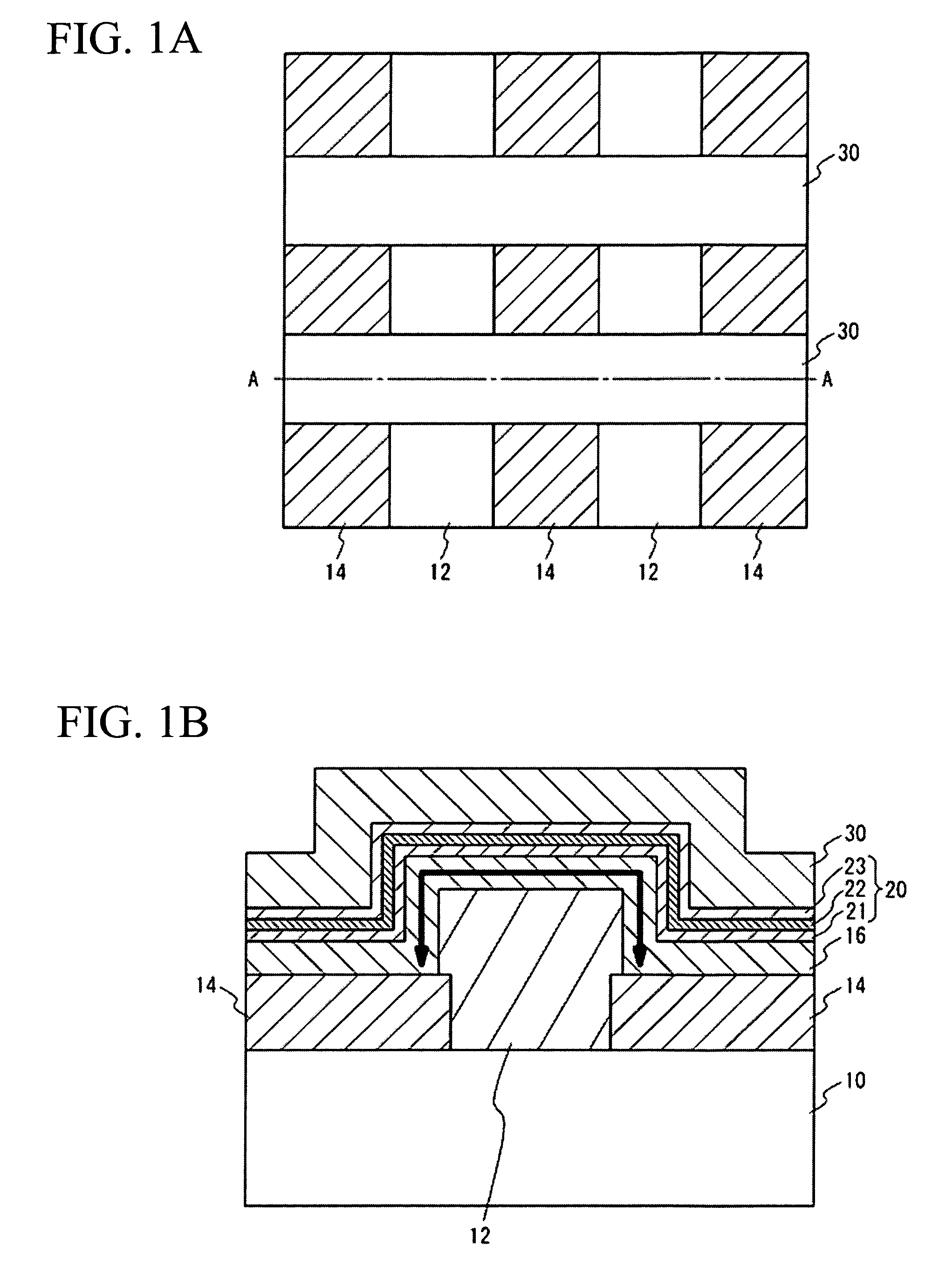
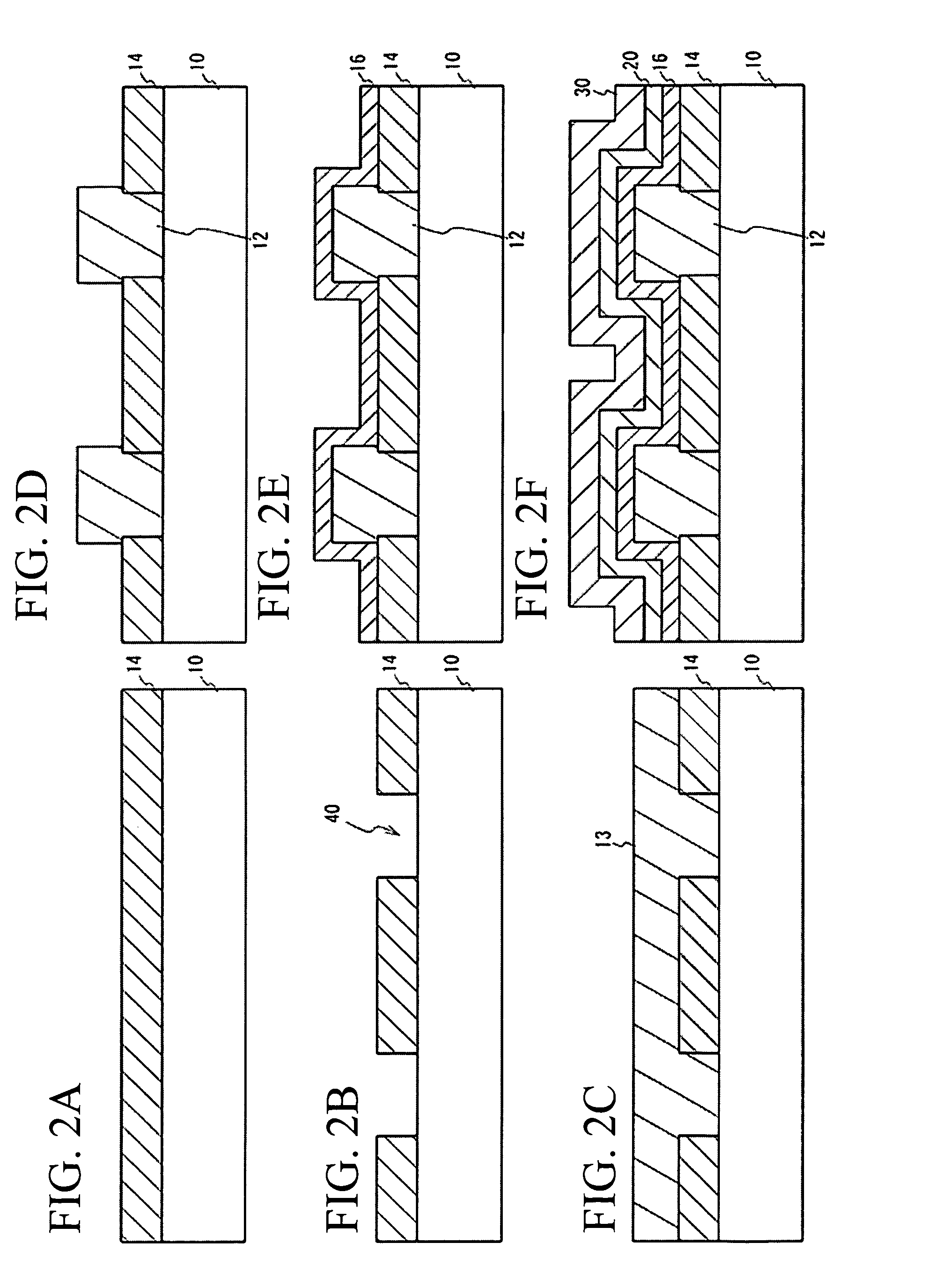
[0040]FIG. 2A through FIG. 2F are cross-sectional views illustrating the procedures for manufacturing the flash memory in accordance with the As shown in FIG. 2A, an n-type polysilicon layer 14 is formed on a substrate 10 such as a quartz substrate, a sapphire substrate, a glass substrate, or a silicon substrate, by chemical vapor deposition (CVD). As shown in FIG. 2B, openings 40 are formed in the polysilicon layer 14 on the substrate 10 by an exposure technique and an etching technique. Through this procedure, the polysilicon layer 14 is turned into bit lines 14. The bit lines 14 are designed to have the same resistivity as the resistivity of the bit lines of a conventional flash memory. As shown in FIG. 2C, a layer 13 to be an insulating layer is formed on and between the bit lines 14. This layer 13 is formed from a silicon oxide film, for example, by CVD.

[0041]As shown in FIG. 2D, etching is performed on predetermined regions of the layer 13 by an exposure technique and an etch...

sixth embodiment

[0053]FIG. 10A through FIG. 10F are cross-sectional views illustrating the procedures for manufacturing the flash memory in accordance with the As shown in FIG. 10A, the substrate 10 such as a quartz substrate, a sapphire substrate, a glass substrate, or a silicon substrate is prepared. As shown in FIG. 10B, etching is performed on predetermined regions of the substrate 10 by an exposure technique and an etching technique, so as to form the insulating layers 12c each having a protruding form on the substrate 10. Although the insulating layers 12c are made of the same material as the substrate 10, the insulating layers 12c are indicated by hatched lines in FIG. 10B through 10F. As shown in FIG. 10C, a layer 17 to be channel layers is formed on the substrate 10 with an n-type polysilicon layer having boron added thereto. The layer 17 covers the insulating layers 12.

[0054]As shown in FIG. 10D, arsenic ions are vertically injected into the portions of the layer 17 to be the channel lay...

eighth embodiment

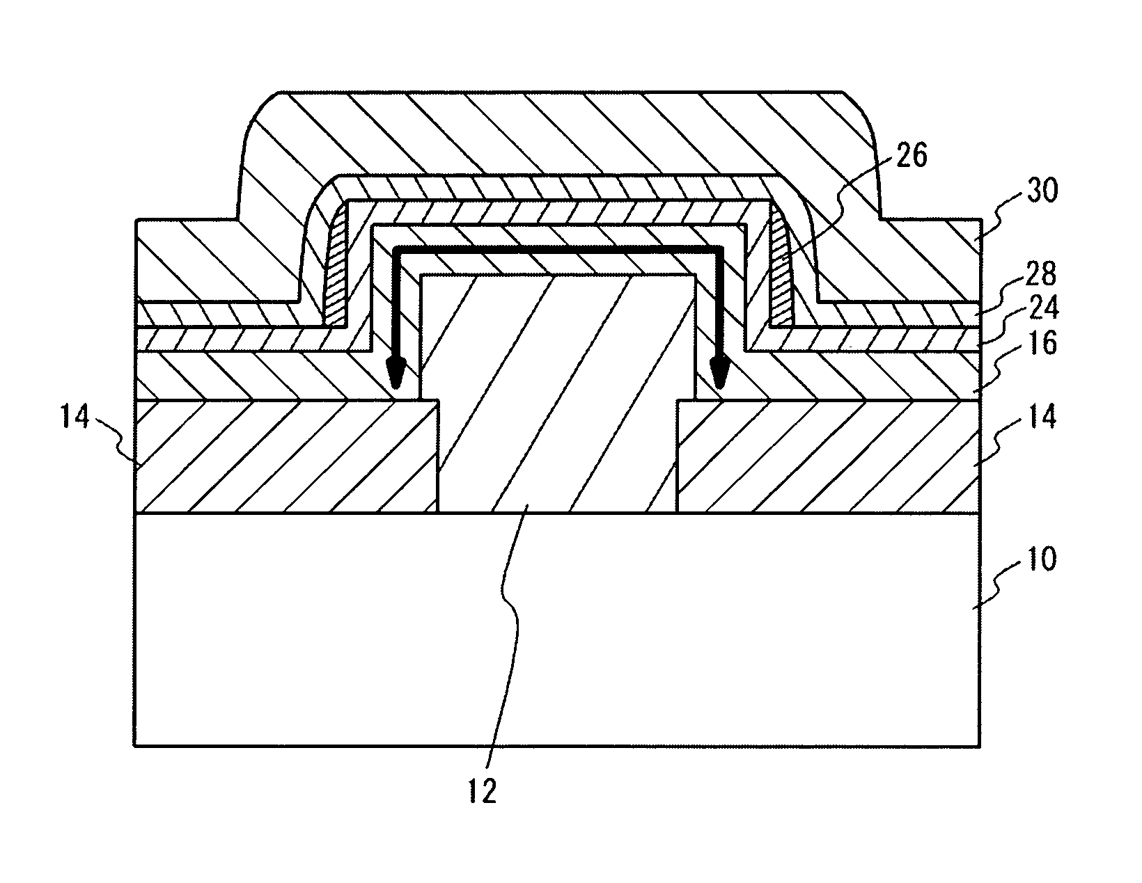
[0060]the present invention is an example case where the substrate has a groove between first bit lines, and an insulating layer is formed in the groove. FIG. 13 is a cross-sectional view of a flash memory in accordance with the eighth embodiment. A groove 11 is formed at the portion of a substrate 10a located between bit lines 14, and the groove 11 is filled with an insulating layer 12d. The other aspects of this structure are the same as those of the sixth embodiment shown in FIG. 9B. The same components as those shown in FIG. 9B are denoted by the same reference numerals as those in FIG. 9B, and explanation of them is omitted herein.

[0061]In the eighth embodiment, the insulating layer 12d is buried at the portion of the substrate 10a located between the bit lines 14. Accordingly, even if the distance between the bit lines 14 is made smaller, the path of a substrate current (indicated by the dotted arrows in FIG. 13) flowing in the substrate 10a can be lengthened between the bit l...


PUM


Abstract

The present invention provides a semiconductor device that has a shorter distance between the bit lines and easily achieves higher storage capacity and density, and a method of manufacturing such a semiconductor device. The semiconductor device includes: first bit lines formed on a substrate; an insulating layer that is provided between the first bit lines on the substrate, and has a higher upper face than the first bit lines; channel layers that are provided on both side faces of the insulating layer, and are coupled to the respective first bit lines; and charge storage layers that are provided on the opposite side faces of the channel layers from the side faces on which the insulating layers are formed.

Description

CLAIM OF PRIORITY[0001]This application claims benefit of priority to under 35 U.S.C. Section 119 from Japanese Patent Application No. JP 2006 / 353415, filed Dec. 27, 2006.TECHNICAL FIELD[0002]This invention relates generally to semiconductor devices and methods of manufacturing the semiconductor devices, and more particularly, to a semiconductor device that has an insulating layer between bit lines, and channel layers on side faces of the insulating layer, and to a method of manufacturing the semiconductor device.BACKGROUND OF THE INVENTION[0003]Recently, non-volatile memories that are data rewritable semiconductor devices have become widely used in the storage of electronic data. In flash memories that are typical of non-volatile memories, transistors forming memory cells have floating gates or insulation films that are known as charge storage layers. In such flash memories, charges are accumulated in the charge storage layers, so as to store data. Studies are still being made to p...

Claims


Application Information

Patent Timeline
Patent Type & Authority Patents(United States)
IPC IPC(8): H01L29/792H01L27/108H01L21/70H01L27/148H01L29/94H01L29/02H01L21/339
CPCH01L21/28273H01L29/788H01L27/115H01L27/11521H01L27/11568H01L29/66825H01L29/66833H01L29/7881H01L29/792H01L29/7926H01L21/28282H01L21/84H01L27/11556H01L27/1203H01L29/42332H01L29/42348H01L29/66757H01L2924/0002H01L29/40114H01L29/40117H10B69/00H10B41/30H10B41/27H10B43/30H01L2924/00H10B41/00H10B43/00H01L23/5283
Inventor HAYAKAWA, YUKIONANSEI, HIROYUKI
Owner MONTEREY RES LLC
Why Eureka
Try Eureka