Polariscope stress measurement tool and method of use

a stress measurement and polariscope technology, applied in the direction of instruments, instruments, force/torque/work measurement apparatus, etc., can solve the problems of increasing residual stresses, introducing additional residual stresses, and unavoidable high thermal gradients at the solid-melt interfa

Inactive Publication Date: 2012-09-11
GEORGIA TECH RES CORP
View PDF3 Cites 17 Cited by
  • Summary
  • Abstract
  • Description
  • Claims
  • Application Information

AI Technical Summary

Benefits of technology

[0110]FIG. 86 illustrates a stress map of the CZ silicon single crystal of FIG. 84 after eliminating system error;

Problems solved by technology

Therefore, a high thermal gradient is unavoidable at the solid-melt interface.
The ensuing thermal processing in cell manufacturing, such as oxidation and diffusion, may also introduce non-uniform heating and cooling that results in a substantial thermal gradient and may introduce additional residual stresses.
In this respect, residual stresses may accelerate or delay the onset of plastic deformation.
In many cases, unexpected failure occurs due to the presence of residual stresses that have combined with the service stresses to shorten component life.
Furthermore, in natural or artificial multiphase materials, residual stresses can result in differences in thermal expansion, yield stress, and stiffness.
Residual stresses in silicon may cause mechanical failure during processing and change the optical or electrical properties of the wafer.
Tensile residual stresses in silicon will lead to crack growth and reduced electron-hole lifetime and wafer breakage.
High tensile stresses will also cause unexpected failure during processing of cells when service stresses are introduced.
Furthermore, the regions close to the wafer edges may contain micro-cracks which will eventually propagate and

Method used


Image

  • Polariscope stress measurement tool and method of use
  • Polariscope stress measurement tool and method of use
  • Polariscope stress measurement tool and method of use

Examples


Embodiment Construction

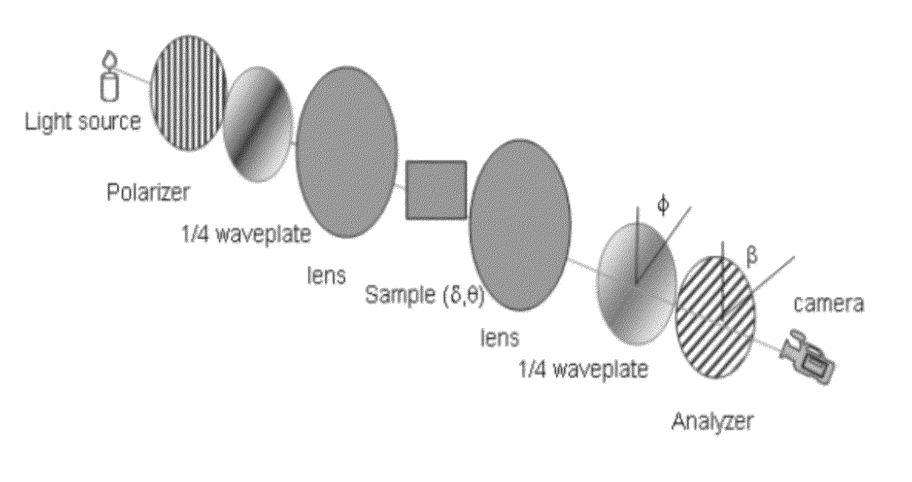
[0113]This instant invention is directed to a tool for and method of measuring stress using a polariscope for thin, flat crystalline solids. Multi-crystal silicon will be discussed herein as a model material. The anisotropic stress optic coefficients are characterized for different crystal and stress orientations. The inventive polariscope system allows for the measurement of large samples. The full stress components are extracted from the measurement of the polariscope by the shear difference method. Finally, the thermally induced stress was modeled using ANSYS and compared to measured stresses.

[0114]In the last number of years, efforts have been made to develop techniques to obtain the in-plane residual stress in silicon, especially in poly-crystalline silicon, in order to improve the efficiency and reliability of photovoltaic cells. Wafers used in the photovoltaic industry are becoming larger and thinner. The residual stresses are generally higher in thin materials, and it takes ...


PUM


Abstract

The present invention provides a tool for and method of using an infrared transmission technique to extract the full stress components of the in-plane residual stresses in thin, multi crystalline silicon wafers including in situ measurement of residual stress for large cast wafers. The shear difference method is used to obtain full stress components by integrating the shear stress map from the boundaries. System ambiguity at the boundaries is resolved completely by introducing a new analytical function. A new anisotropic stress optic law is provided, and stress optic coefficients are calibrated for different crystal grain orientations and stress orientations.

Description

CROSS-REFERENCE TO RELATED APPLICATIONS[0001]This patent application claims the benefit of U.S. Provisional Patent Application No. 61 / 485,401 filed on May 12, 2011, which is incorporated herein by reference in its entirety.BACKGROUND OF THE INVENTION[0002]1. Field of the Invention[0003]The present invention relates to a tool for and method of measuring, and, more particularly, the present invention relates to in situ, non-destructive determination of the full stress components for thin, flat crystalline solids using poliariscopy.[0004]2. Description of the Related Art[0005]The photovoltaic (PV) industry uses single crystal and polycrystalline silicon in the manufacturing of PV modules. Single crystal wafers are usually grown from a liquid melt into ingots by the Czochralski (CZ) method as shown in FIG. 1. The Czochralski method is used for high volume production of single crystal silicon. A crystal is “pulled” out of a vessel containing liquid silicon by dipping a seed crystal into ...

Claims


Application Information

Patent Timeline
IPC IPC(8): G01B11/16G01J4/00
CPCG01B11/168G01L5/0047G01L1/241
Inventor DANYLUK, STEVENLI, FANG
Owner GEORGIA TECH RES CORP
Why Eureka
Try Eureka