Optical waveguide element, chromatic dispersion compensator, methods for designing chromatic dispersion compensator, optical filter, methods for designing optical filter, optical resonator and methods for designing optical resonator

a technology of chromatic dispersion compensator and optical waveguide element, which is applied in the direction of optical elements, multiplex communication, instruments, etc., to achieve the effect of reducing manufacturing cost, improving manufacturing yield, and easy tolerability control in the manufacturing process

Inactive Publication Date: 2012-09-18
THE FUJIKURA CABLE WORKS LTD
View PDF47 Cites 11 Cited by
  • Summary
  • Abstract
  • Description
  • Claims
  • Application Information

AI Technical Summary

Benefits of technology

[0057]According to the exemplary aspect described in (1) above, compared with a conventional chirped-type grating in which the pitch changes gradually, tolerance control in the manufacturing process is easier and this contributes to an improvement in the manufacturing yield.
[0058]According to the exemplary aspect described in (2) above, it is possible to make the waveguide length shorter than in a sampled grating.
[0059]According to the exemplary aspect described in (3) above, because the confinement of light in an inner side core which is formed from a high refractive index material is weaker, compared to a conventional embedded type of optical waveguide with high relative refractive index difference which is only formed from two portions, namely, a core and a cladding which are formed from high refractive index materials, it is possible to inhibit the effects (i.e., scattering loss) on the optical characteristics from roughness on the inner-side core side walls, in which the roughness is unavoidably generated in the manufacturing process.
[0060]According to the exemplary aspect described in (4) above, because the mode field diameter of the fundamental mode expands, it is possible to inhibit the effects (i.e., scattering loss) on the optical characteristics from roughness on the inner-side core side walls which is unavoidably generated in the manufacturing process.
[0061]According to the exemplary aspect described in (5) above, in a planar optical waveguide element having a Bragg grating pattern, it is possible to reduce the polarization dependence of the optical characteristics.
[0062]According to the exemplary aspect described in (6) above, because a small-sized chromatic dispersion compensator that collectively compensates chromatic dispersion and dispersion slopes in a plurality of channels can be achieved by a Bragg grating structure having pitches (local period) to which only a limited small number of, namely, three or more different discrete values have been assigned, in the manufacturing process of an element or phase mask, control of the fabrication accuracy is easier and this contributes to an improvement in the manufacturing yield.

Problems solved by technology

However, in the fiber Bragg grating, because there are limits to the range over which the refractive index can be changed in order to manufacture a grating pattern, an operation in which the aforementioned spectrum characteristics are apodized by applying an inverse Fourier transform is also carried out so that these limits are not exceeded.

Method used


Image

  • Optical waveguide element, chromatic dispersion compensator, methods for designing chromatic dispersion compensator, optical filter, methods for designing optical filter, optical resonator and methods for designing optical resonator
  • Optical waveguide element, chromatic dispersion compensator, methods for designing chromatic dispersion compensator, optical filter, methods for designing optical filter, optical resonator and methods for designing optical resonator
  • Optical waveguide element, chromatic dispersion compensator, methods for designing chromatic dispersion compensator, optical filter, methods for designing optical filter, optical resonator and methods for designing optical resonator

Examples


first embodiment

of an Optical Waveguide Element

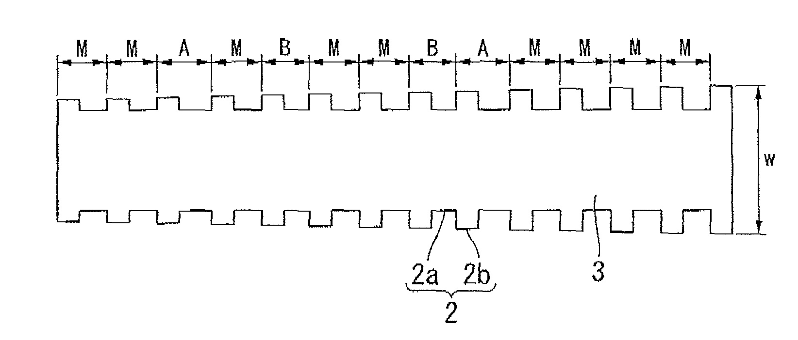
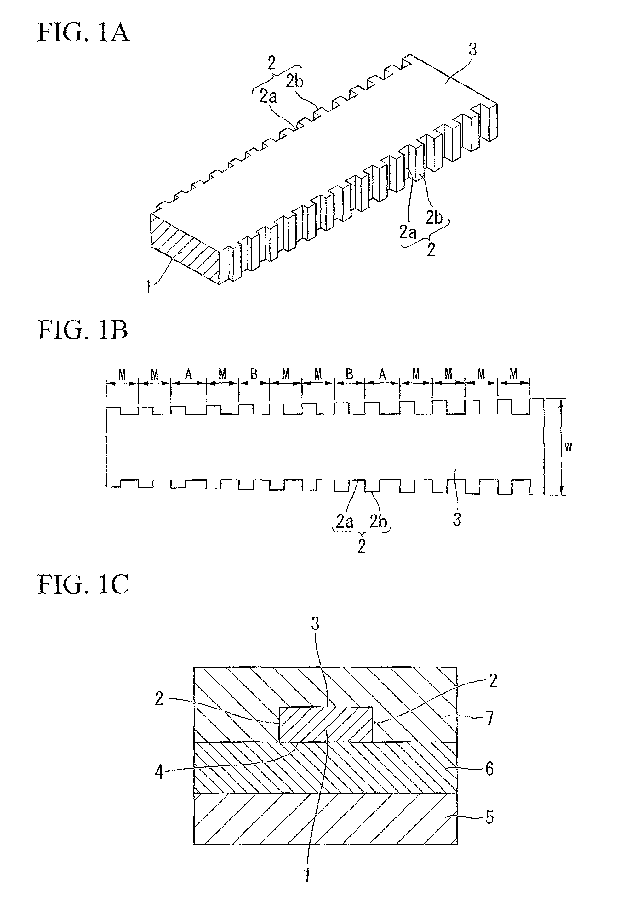
[0173]A first exemplary embodiment of the optical waveguide element is shown in typical view in FIG. 1A through FIG. 1C. FIG. 1A is a perspective view of a portion of a core 1 of an optical waveguide, FIG. 1B is a plan view of the same portion of the core 1, and FIG. 1C is a cross-sectional view of an optical waveguide element. This optical waveguide element is a planar optical waveguide element in which an optical waveguide is formed on a substrate 5. The optical waveguide comprises a bottom cladding 6 which is formed on the substrate 5, a core 1 that is formed on the bottom cladding 6, and a top cladding 7 that is formed on the core 1 and on the bottom cladding 6. The grating structure comprises recessed portions 2a and protruding portions 2b that are formed in both side walls of the core 1 as periodical changes in the width w of the core 1. A top surface 3 and bottom surface 4 of the core 1 are flat.

[0174]In a high-function element such as a chromat...

second embodiment

of Optical Waveguide Element

[0191]An example of an optical waveguide element of the second embodiment of the present invention is shown in FIG. 3A through FIG. 3C. The optical waveguide element is a planar optical waveguide element in which an optical waveguide is located on the substrate. If the width or thickness of the waveguide in the light propagation direction is changed periodically in an optical waveguide, then the effective refractive index of the optical waveguide also changes periodically, and a Bragg grating can be constructed. In FIG. 3A through FIG. 3C, only the core 10 is shown and the claddings are not shown, however, it is to be assumed that cladding surrounds the periphery of the core 10. In addition, a substrate (not shown) is located below the cladding, and a bottom surface 14 of the core; 10 is parallel with the substrate surface. The term “horizontal direction” refers to a direction which is parallel to this substrate surface, and the term “vertical direction” ...

third embodiment

of an Optical Waveguide Element

[0216]An optical wave guide having a cross-sectional structure such as that shown in FIG. 7 can be given as an example of a Bragg grating optical waveguide structure in which polarization dependence has been reduced. On account of the simplified description of the principle of reducing polarization dependence, the cross-sectional structures of the cores 10 are all the same in, the planar optical waveguide elements of FIGS. 3A through 3C and FIGS. 6A through 6C. However, if the effective refractive index is changed by changing the dimensions of the optical waveguide, then an optical waveguide having a composite core structure such as that shown in FIG. 7 is preferable in order to improve the accuracy of the effective refractive index.

[0217]The core of the planar optical waveguide element 20 having the cross-sectional structure shown in FIG. 7 is a composite core formed by two areas, namely, inner side cores 21 and 22 and an outer side core 24.

[0218]In t...


PUM

PropertyMeasurementUnit
refractive indexaaaaaaaaaa
grating lengthaaaaaaaaaa

Abstract

There is provided an optical waveguide element comprises: a core of an optical waveguide; and a Bragg grating pattern that is provided on the core, wherein a pitch of the Bragg grating pattern takes a value from among three or more predetermined discrete values; the pitches that take the respective discrete values are present in a plurality of locations over an entire length of the optical waveguide respectively; and if a value from among all of the discrete values which has the highest distribution frequency is taken as M, and if the closest value to the M which is larger than the M is taken as A, and if the closest value to the M which is smaller than the M is taken as B, then a difference expressed as A−M is equal to a difference expressed as M−B.

Description

CROSS-REFERENCE TO RELATED APPLICATION[0001]This is a Continuation Application of International Application No. PCT / JP2009 / 053731, filed on Feb. 27, 2009, which claims priority to Japanese Patent Application No. 2008-049841, filed Feb. 29, 2008. The contents of the aforementioned applications are incorporated herein by reference.TECHNICAL FIELD[0002]Description herein related to an optical waveguide element which has a Bragg grating pattern, and which can be used in various applications such as a chromatic dispersion compensator, an optical filter and an optical resonator and the like, and also related to a design method thereof.BACKGROUND ART[0003]The following are examples of chromatic dispersion compensation in an optical waveguide structure for which polarization dependence is not considered.[0004]A dispersion compensator which has a Bragg grating pattern on the waveguide is disclosed in Patent document 1. The dispersion compensator disclosed in Patent document 1 has a plurality...

Claims


Application Information

Patent Timeline
Patent Type & Authority Patents(United States)
IPC IPC(8): G02B6/34H01B3/00H04J14/02
CPCG02B6/12007G02B6/124G02B6/29394G02F1/225G02F2001/213G02F2201/02G02F2201/307G02F1/213
Inventor OGAWA, KENSUKEGUAN, NINGSAKUMA, KEN
Owner THE FUJIKURA CABLE WORKS LTD
Why Eureka
Try Eureka