Nitride semiconductor substrate and manufacturing method of the same

a technology of nitride and semiconductor substrate, which is applied in the direction of crystal growth process, polycrystalline material growth, chemically reactive gas growth, etc., can solve the problems of low production yield of substrate, difficult to obtain high-quality growth layer, and non-uniform warpage shape of substrate, so as to improve the production yield of the device

Active Publication Date: 2012-09-25
SUMITOMO CHEM CO LTD
View PDF12 Cites 0 Cited by
  • Summary
  • Abstract
  • Description
  • Claims
  • Application Information

AI Technical Summary

Problems solved by technology

Therefore, it is difficult to obtain a high quality growth layer, and a plurality of crystal defects are contained in the obtained nitride semiconductor layer.
However, even when the method for forming this low temperature deposition buffer layer is used, tremendous degree of crystal defects such as threading dislocations and vacancy exist in the obtained GaN film, and therefore it is insufficient in this method, to obtain an element having high performance which is desired at present.
Therefore, it is absolutely difficult to suppress generation of the dislocations low, in the vicinity of an interface of heteroepitaxial growth at initial time of the crystal growth.
Therefore, the substrate takes a non-uniform warpage shape.
However, a substrate rear surface can not be tightly adhered to the substrate holder, due to the warpage of the substrate.
Therefore, a temperature distribution is generated in the substrate, and as a result, a uniform-film thickness distribution can not be obtained in the epitaxial film formed on the substrate surface.
However, in manufacturing the substrate holder with high dimension accuracy, most of the substrate holders have a uniform warpage shape symmetrical with respect to a center, and it is extremely difficult to manufacture the substrate holder having the non-uniform warpage shape, with high accuracy.
Therefore, when non-uniformity of the warpage shape of the substrate is great, the substrate holder and the substrate rear surface are not adhered to each other, in a case of the substrate holder having the uniform warpage shape symmetrical with respect to the center, thus allowing a non-uniform temperature distribution to be generated and the uniform film thickness distribution can not be obtained.
Further, even if the substrate holder having the non-uniform warpage shape equivalent to that of the substrate rear surface can be manufactured with high accuracy, there is a problem that cost is incurred in manufacture, and further the substrate holder must be exchanged within the specific number of times, due to deterioration of the substrate holder in each growth, thus incurring much cost.
Note that this problem is involved not only in the GaN freestanding substrate, but also in other nitride semiconductor substrate.

Method used


Image

  • Nitride semiconductor substrate and manufacturing method of the same
  • Nitride semiconductor substrate and manufacturing method of the same
  • Nitride semiconductor substrate and manufacturing method of the same

Examples


example 1

[0071]The GaN base layer having a thickness of 300 nm was formed on the sapphire substrate having a diameter of 2.5 inch, by the MOVPE method using the MOVPE apparatus shown in FIG. 5. As growth conditions, trimethyl gallium (TMG) was used as the organic metal raw material, NH3 gas was used as the gas raw material, and the H2 gas and N2 gas were used as the carrier gas.

[0072]Flow rate TMG: 100 sccm, NH3: 30 liter / min, H2: 75 liter / min, N2: 50 liter / min

[0073]Temperature 1100° C.

[0074]Pressure 300 Torr

[0075]Growth time 3 minutes

[0076]wherein, the substrate holder with no warpage was used, because the GaN layer was formed on the sapphire substrate with no warpage.

[0077]Ti having a thickness of 20 nm was deposited on the front surface of the GaN base layer, then heat treatment was applied thereto for 30 minutes at 1,000° C. in the mixture flow, to thereby manufacture the void formed substrate having a net-like TiN film (for example, see Japanese Patent Laid Open Publication No. 2003-178...

example 2

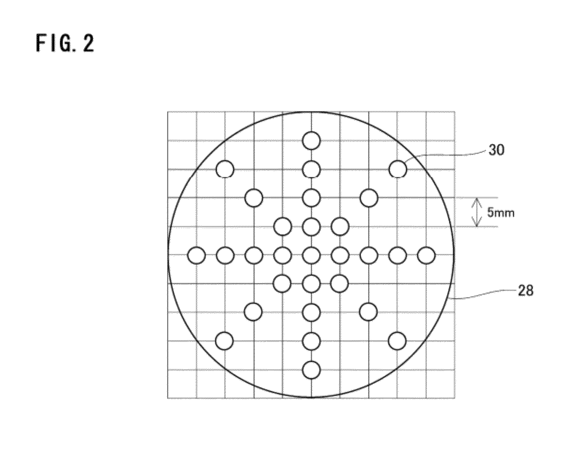
[0083]A single layer film was epitaxyally-grown by using the GaN substrate obtained in the example 1, and its film thickness distribution was examined.

[0084]By using the GaN substrate of samples No. 1 to 13, the single layer of AlGaN was grown by the MOVPE method using the MOVPE apparatus shown in FIG. 5. As the growth conditions, trimethyl gallium (TMG) and trimethyl aluminum (TMA) were used as organic metal raw materials, the NH3 gas was used as the gas raw material, and the H2 gas and N2 gas were used as the carrier gas.

[0085]Flow rate TMG: 100 sccm, TMA: 100 sccm, NH3: 30 liter / min, H2: 75 liter / min, N2: 50 liter / min, temperature: 1,000° C., Pressure: 300 Torr, Growth time 120 minutes.

[0086]Further, the substrate holder was set to have the warpage amount corresponding to the values of Have of each one of the samples No. 1 to 13, and the substrate holder having a uniform warpage shape symmetrical with respect to its center was used.

[0087]The single layer of AlGaN having compositi...


PUM

PropertyMeasurementUnit
temperatureaaaaaaaaaa
thicknessaaaaaaaaaa
diameteraaaaaaaaaa

Abstract

To improve an adhesion to a substrate holder, and improve a device production yield by uniformizing a temperature distribution in a surface of a substrate and uniformizing characteristics such as a film thickness. When a concave warpage is set to be negative on a substrate front side, and a convex warpage is set to be positive on the substrate front side, then a line segment is drawn from one end of a substrate rear surface to the other end of the substrate rear surface, passing through a substrate center line, and a substrate is sliced by this line segment in a substrate thickness direction, a maximum value of shortest values of a distance from an arbitrary point on the drawn line segment to a rear side outline in a sliced surface, is defined as warpage H in a diameter direction, and when the warpage H in the diameter direction is obtained in a substrate peripheral direction, with its maximum value set to be Hmax, and its minimum value set to be Hmin, the warpage H in the diameter direction is defined to satisfy Hmax−Hmin≦30 μm.

Description

BACKGROUND[0001]1. Technical Field[0002]The present invention relates to a nitride semiconductor substrate and a manufacturing method of the same, and particularly suitably relates to a gallium nitride substrate.[0003]2. Description of Related Art[0004]Group III-V nitride semiconductor materials such as gallium nitride (GaN), indium gallium nitride (InGaN), gallium aluminium nitride (GaAlN) have a sufficiently large forbidden band width, and an inter-band transition is a direct transition type. Therefore, examination is actively performed, regarding an application to a short-wavelength light emitting element. Also, application to an electronic element is also expected, because a saturation drift velocity of electrons is great, and 2-dimensional carrier gas by hetero-junction can be utilized.[0005]A nitride semiconductor layer constituting these elements can be obtained by causing epitaxial growth on a base substrate, by using vapor-phase deposition methods such as a metal-organic va...

Claims


Application Information

Patent Timeline
Patent Type & Authority Patents(United States)
IPC IPC(8): H01L29/20
CPCC30B25/02C30B29/406H01L21/0242H01L21/02458H01L21/0254H01L21/0262Y10T83/0405
Inventor YAMAMOTO, SHUNSUKE
Owner SUMITOMO CHEM CO LTD
Why Eureka
Try Eureka