Solid state imaging device for correcting level variations in output signals

a level variation and output signal technology, applied in exposure control, radio frequency controlled devices, instruments, etc., can solve the problems of device generation of horizontal stripe noise, cmos sensor may not be able to perform the correction, horizontal stripe noise, etc., to achieve short exposure time, high sensitivity, and correct level variation flicker

Inactive Publication Date: 2012-10-09
FUNAI ELECTRIC CO LTD
View PDF11 Cites 4 Cited by
  • Summary
  • Abstract
  • Description
  • Claims
  • Application Information

AI Technical Summary

Benefits of technology

[0022]It is an object of the present invention to provide a solid state imaging device with simple and inexpensive configuration that can reduce or correct level variation of output signals (variation in the amount of output signals) caused by variation in the amount of energy of illumination when imaging, using a solid state imaging element such as a CMOS sensor, under discharge type illumination e.g. with high luminance.
[0025]Thus, according to this solid state imaging device using the X-Y address type imaging element, it is possible to prevent output signals of the imaging element from varying in amplitude corresponding to the period of energy variation of the illumination (i.e. it is possible to correct level variation and flicker), even if discharge type illumination is used for the illumination under which imaging is performed, and even if the exposure time (total exposure time) is shorter than the period of energy variation of the discharge type illumination. As a result, normal images can be obtained even if imaging is performed with high sensitivity (imaging with a short exposure time) under discharge type illumination e.g. of a fluorescent lamp. Accordingly, the X-Y address type solid state imaging element (CMOS sensor) can be used in place of a CCD sensor as a two-dimensional image sensor in the solid state imaging device such as a camcorder which mainly handles moving images. The solid state imaging device according to the present invention can correct the level variation and flicker basically under any illumination such as high frequency illumination so as to obtain normal images.
[0026]Preferably, the variation detecting means uses a light receiving element such as a photodiode, placed to face an object to be captured, for detecting the period of energy variation of the discharge type illumination. This makes it possible to more securely detect the period (frequency) of energy variation of the illumination, achieving more secure performance of the solid state imaging device, including setting of the total exposure time matched to the period of energy variation of the illumination.
[0027]Further preferably, the variation detecting means detects the period of energy variation of illumination based on an output signal of the imaging element in which the output signal of the imaging element contains energy variation components of the light source, the energy variation components of the light source being held for a predetermined time. The use of the imaging element for the detection of the illumination energy variation period makes it possible to eliminate the need for another detector such as a photodiode for the detection, and thereby reduce the number of components in the solid state imaging device, reducing the size and cost.

Problems solved by technology

However, this causes a problem that when correcting or significantly reducing level variations in output signals from an imaging device using a CMOS sensor, a conventional correction method to adjust the exposure time of an electronic shutter to the period of the field or frame frequency of the CMOS sensor may not be able to perform the correction.
This causes output signals varying in level or amplitude for each scan line, whereby so-called horizontal stripe noise occurs in the resultant image data from the imaging device.
If such signals with the level variation are output from an imaging device, resultant image data from the imaging device generates horizontal stripe noise such that bright horizontal stripes and dark horizontal stripes appear in an alternating sequence in the scan lines.
However, the conventional correction method has a limitation in the ability to correct the level variation of output signals if the CMOS sensor has improved sensitivity to cause short exposure time as described above.
As a result, the level variation of the output signals occurs which cannot be corrected or significantly reduced by the conventional correction method, causing low quality of images taken by the imaging device.
Accordingly, the method for correcting the level variation and flicker in the CCD sensor cannot be used in the same manner for the CMOS sensor.
Further, the level variation of the CMOS sensor increases with the increase of the luminance, so that the CMOS sensor has been considered unsuitable for use as a sensor in a solid state imaging device such as a digital camera which requires high sensitivity.
This correction method of Japanese Laid-open Patent Publication 2003-032551 is disadvantageous in that the period of energy variation of the illumination is not related to the length of the exposure time.
However, if the exposure time is not an integer multiple of the illumination frequency, the amount of the integrated signal charges to be output is not constant.
Accordingly, although it may be possible to reduce the level variation and flicker to some extent, it is not possible to correct or eliminate them.
However, a problem arises in the driving method of Japanese Laid-open Patent Publication Hei 6-253216 if it is used with a CMOS sensor.
However, a problem of complexity in device configuration arises in the imaging device of this patent publication.
This causes the imaging device and its process to inevitably be complex and costly (e.g. cost increase due to the increase of external memories).

Method used


Image

  • Solid state imaging device for correcting level variations in output signals
  • Solid state imaging device for correcting level variations in output signals
  • Solid state imaging device for correcting level variations in output signals

Examples


Embodiment Construction

[0045]Embodiments of the present invention, as best mode for carrying out the invention, will be described hereinafter with reference to the drawings. The present invention relates to a solid state imaging device which can correct or significantly reduce level variation and flicker. It is to be understood that the embodiments described herein are not intended as limiting, or encompassing the entire scope of, the present invention. Note that like parts are designated by like reference numerals or characters throughout the drawings.

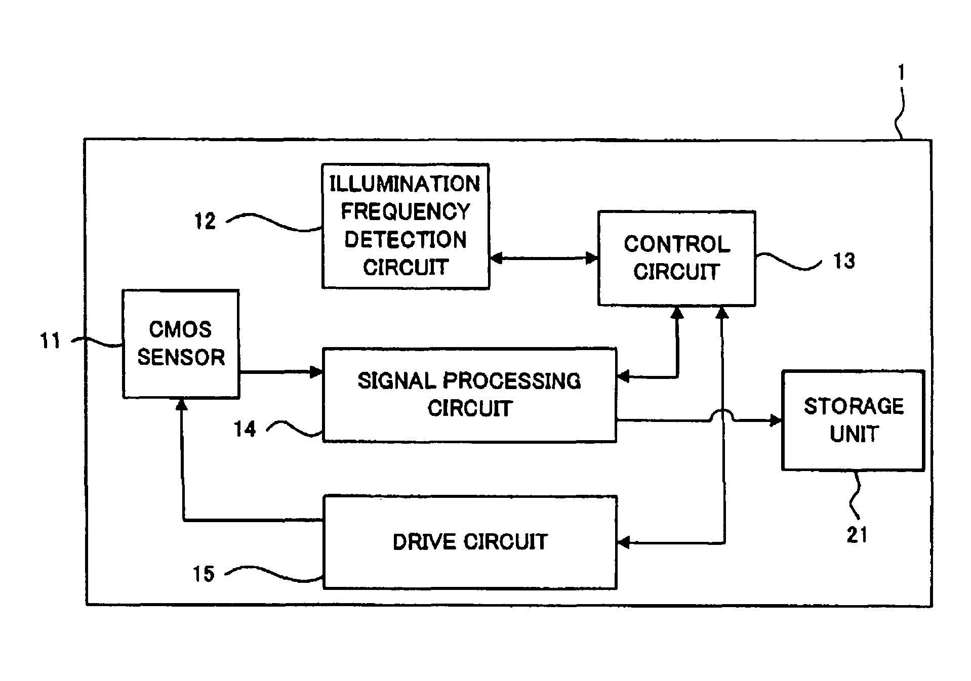
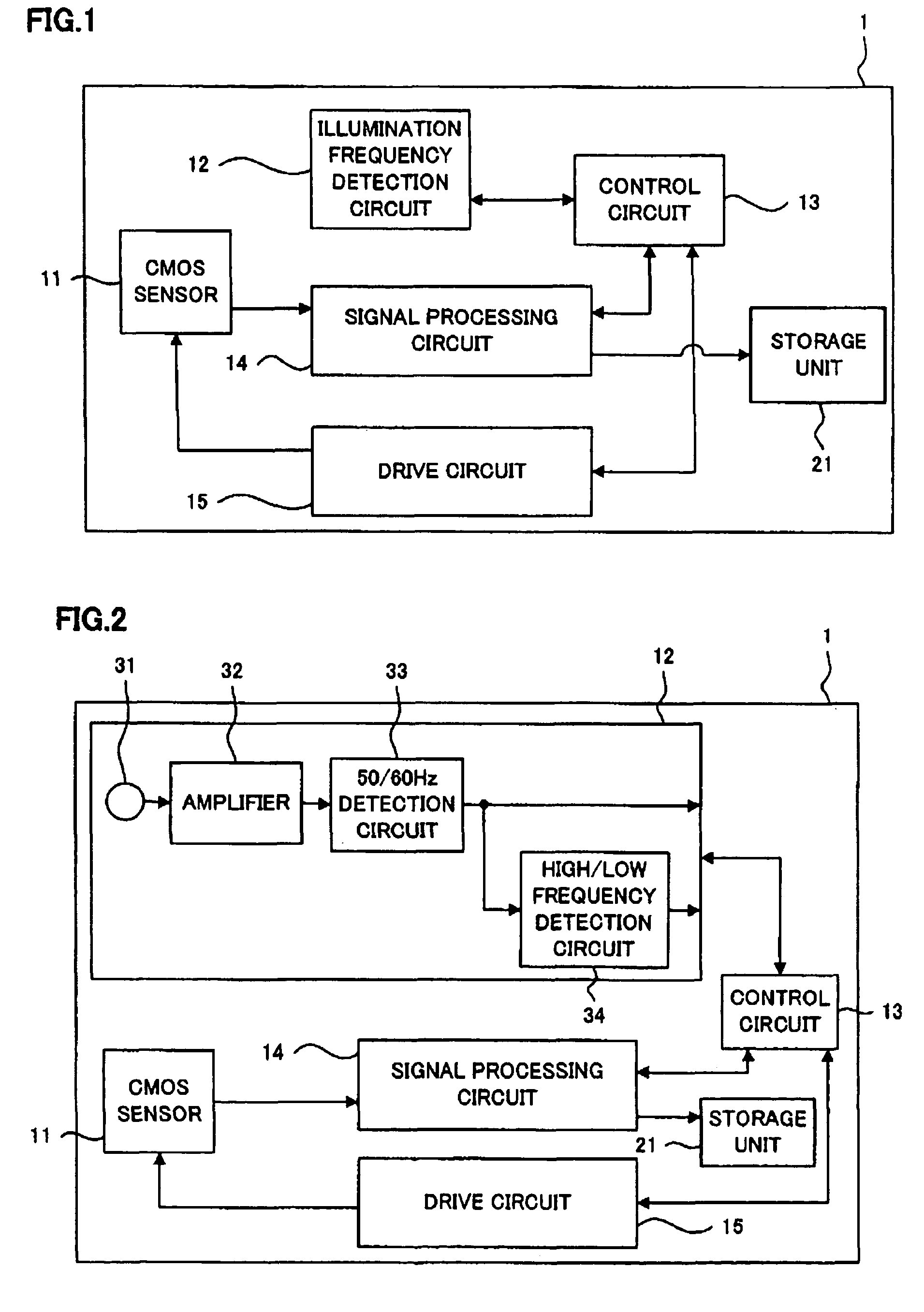
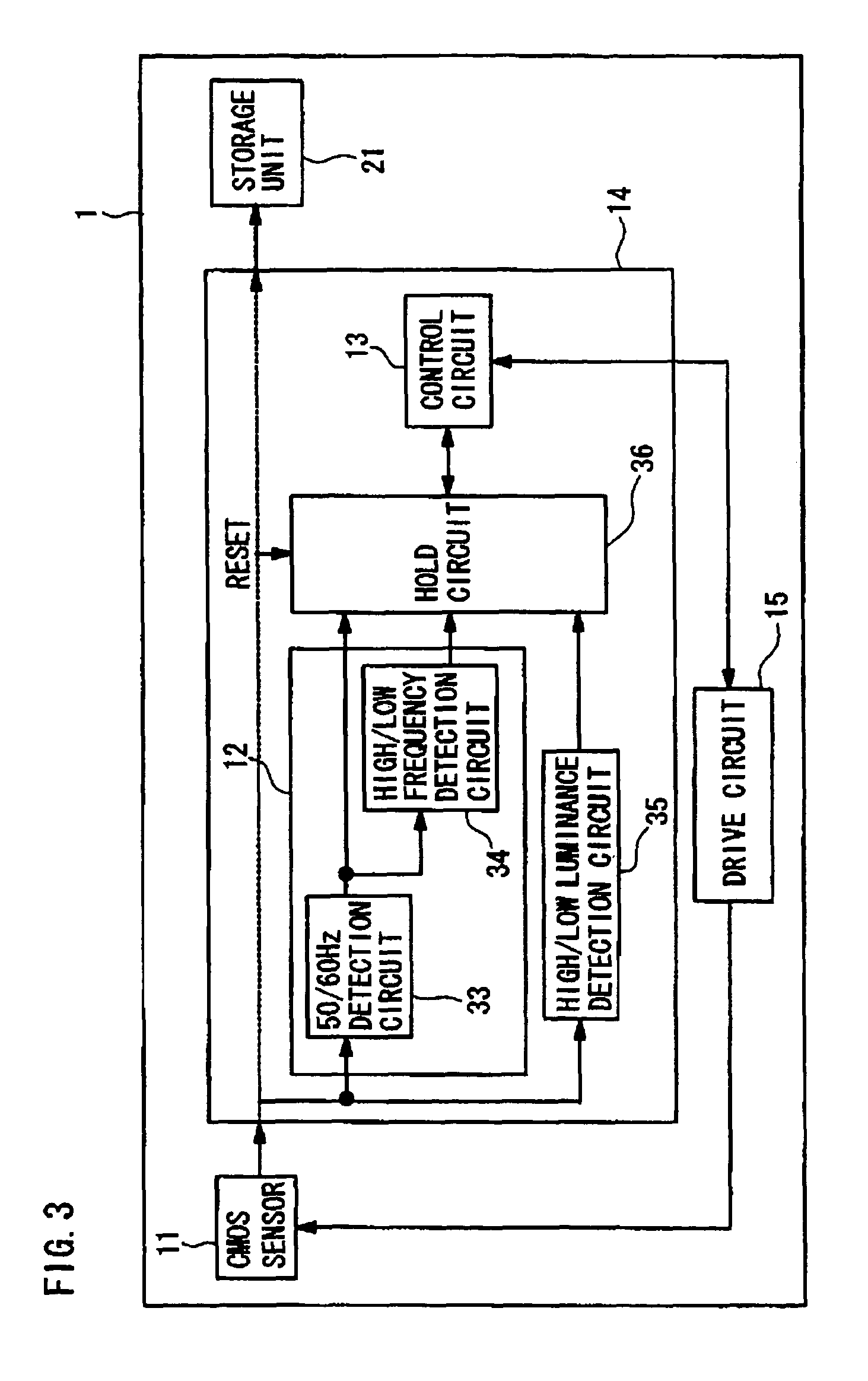
[0046]FIG. 1 is a schematic block diagram of an example of an electrical circuit of a solid state imaging device 1 according to the present invention. As shown in FIG. 1, the solid state imaging device 1 comprises a CMOS (Complementary Metal Oxide Semiconductor) sensor 11, an illumination frequency detection circuit 12, a control circuit 13, a signal processing circuit 14, a drive circuit 15 and a storage unit (memory) 21.

[0047]The CMOS sensor 11 is an imag...


PUM


Abstract

A solid state imaging device detects the period of energy variation of discharge type illumination, and sets a total exposure time to match the detected period. The total exposure time is divided into alternating valid and invalid exposure times by a division ratio to make the sum of the valid exposure times equal to an actual exposure time corresponding to an actual speed of an electronic shutter. Charges accumulated in a CMOS sensor during the valid exposure times are stored in a floating diffusion, whereas charges accumulated during the invalid exposure times are drained. At the end of the total exposure time, the charges stored during the valid exposure times are converted to an electrical signal which is output to a signal processing circuit. This device can correct variation of output signals which corresponds to the illumination energy variation when the shutter is operated for imaging under high luminance illumination.

Description

BACKGROUND OF THE INVENTION[0001]1. Field of the Invention[0002]The present invention relates to a solid state imaging device, more particularly to a technology for correcting level variations in output signals from a solid state imaging device using an X-Y address type solid state imaging element for sequentially reading out pixel signals from pixels by X-Y addressing.[0003]2. Description of the Related Art[0004]A CCD (Charge Coupled Device) sensor and a CMOS (Complementary Metal Oxide Semiconductor) sensor are widely known as solid state imaging elements to be used for imaging devices such as a video camera and a digital camera. Among them, recently, the CMOS sensor has tremendously been improved in sensitivity. However, this causes a problem that when correcting or significantly reducing level variations in output signals from an imaging device using a CMOS sensor, a conventional correction method to adjust the exposure time of an electronic shutter to the period of the field or ...

Claims


Application Information

Patent Timeline
Patent Type & Authority Patents(United States)
IPC IPC(8): H04N5/235H01L27/146H04N5/335H04N5/351H04N5/353H04N5/357H04N5/369H04N5/374H04N5/376
CPCH04N5/2351H04N5/2353H04N23/71H04N23/73
Inventor TANAKA, HIROMICHIYOSHIMURA, HIDETOTERAKAWA, SUMIOKIMATA, MASAFUMI
Owner FUNAI ELECTRIC CO LTD
Why Eureka
Try Eureka