Organic EL device

a technology of organic el and el-based dyes, which is applied in the direction of discharge tube luminescnet screens, anthracene dyes, methine/polymethine dyes, etc., can solve the problems of short life of cbp, inapplicability to devices, and inefficient transfer of energy to the dopan

Active Publication Date: 2012-10-23
IDEMITSU KOSAN CO LTD
View PDF50 Cites 26 Cited by
  • Summary
  • Abstract
  • Description
  • Claims
  • Application Information

AI Technical Summary

Benefits of technology

[0029]Moreover, in order for the dopant to sufficiently emit, extra load (e.g., increasing voltage) is required to be applied on the device, resulting in shortening emission lifetime.
[0438]Specifically, a preferable reduction-causing dopant is at least one alkali metal selected from a group of Li (work function: 2.9 eV), Na (work function: 2.36 eV), K (work function: 2.28 eV), Rb (work function: 2.16 eV) and Cs (work function: 1.95 eV), or at least one alkali earth metal selected from a group of Ca (work function: 2.9 eV), Sr (work function: 2.0 to 2.5 eV) and Ba (work function: 2.52 eV). The reduction-causing dopant having work function of 2.9 eV or less is particularly preferable. Among the above, a more preferable reduction-causing dopant is at least one alkali metal selected from a group of K, Rb and Cs. A further more preferable reduction-causing dopant is Rb or Cs. The most preferable reduction-causing dopant is Cs. Since the above alkali metals have particularly high reducibility, addition of a relatively small amount of these alkali metals to an electron injecting zone can enhance luminance intensity and lifetime of the organic EL device. As a reduction-causing dopant having work function of 2.9 eV or less, a combination of two or more of the alkali metals is also preferable. Particularly, a combination including Cs (e.g., Cs and Na, Cs and K, Cs and Rb, or Cs, Na and K) is preferable. A reduction-causing dopant containing Cs in a combining manner can efficiently exhibit reducibility. Addition of the reduction-causing dopant to the electron injecting zone can enhance luminance intensity and lifetime of the organic EL device.

Problems solved by technology

However, CBP may exhibit short lifetime depending on a layer arrangement of the organic EL device, and thus may not be practically applicable for the device.
When CBP is used as the fluorescent host, energy is not efficiently transferred to the dopant since a difference in singlet energy gap between CBP and the fluorescent material as the dopant is excessively large.

Method used


Image

  • Organic EL device
  • Organic EL device
  • Organic EL device

Examples


example 1

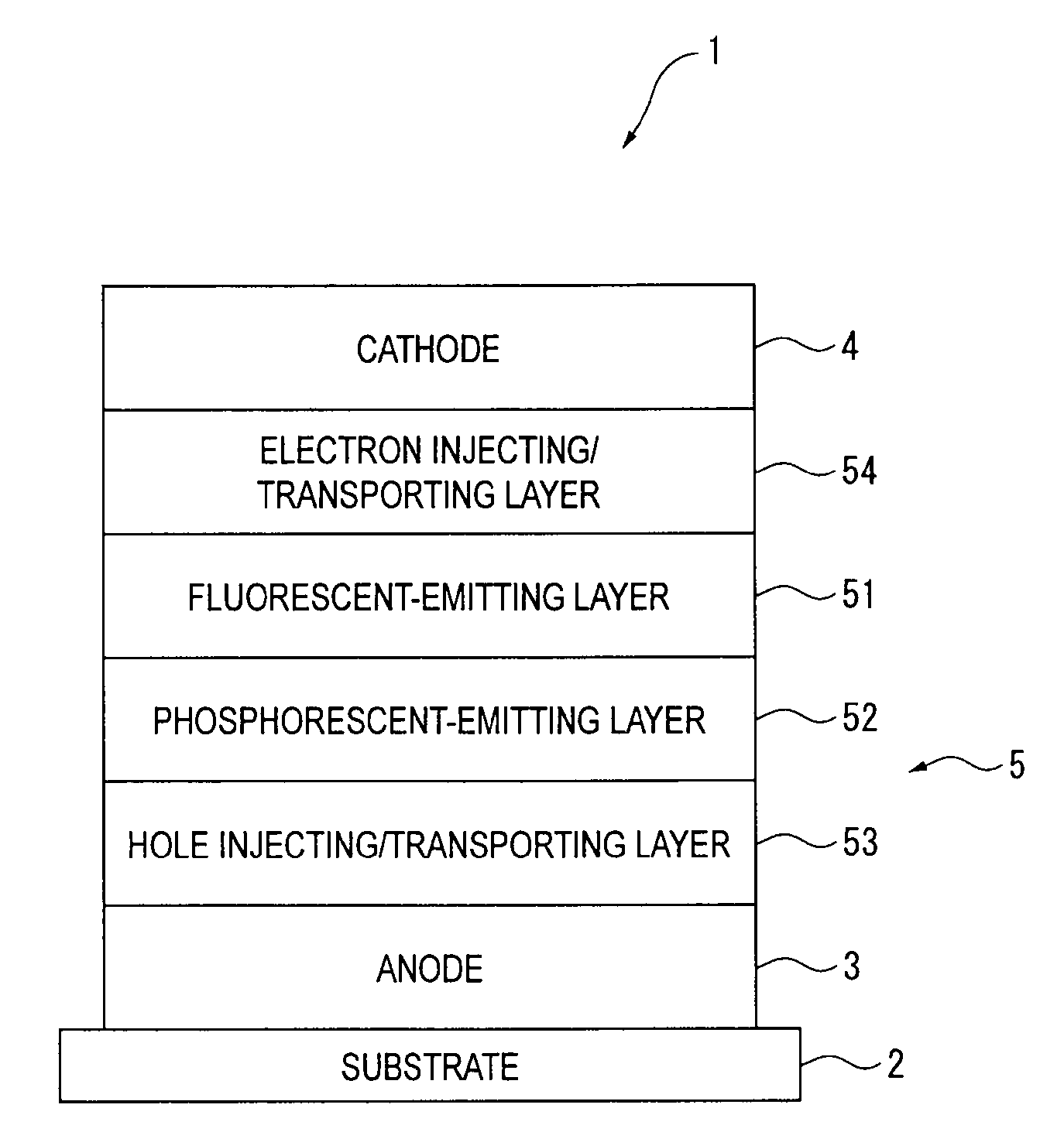
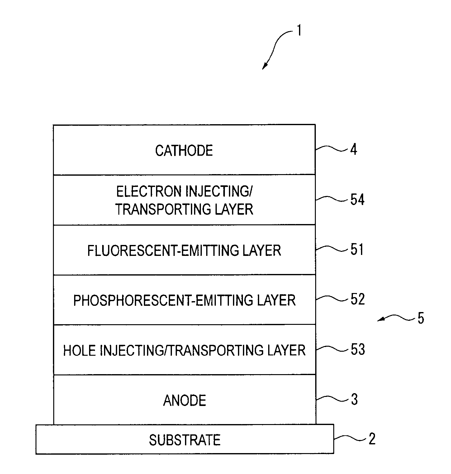
[0461]A glass substrate (size: 25 mm×75 mm×1.1 mm thick) having an ITO transparent electrode (manufactured by Geomatec Co., Ltd.) was ultrasonic-cleaned in isopropyl alcohol for five minutes, and then UV / ozone-cleaned for 30 minutes.

[0462]After the glass substrate having the transparent electrode line was cleaned, the glass substrate was mounted on of a substrate holder of a vacuum deposition apparatus. Then, 55-nm thick film of 4,4′-bis[N-(1-naphthyl)-N-phenylamino]biphenyl (hereinafter abbreviated as “NPD film”) was initially formed by resistance heating deposition onto a surface of the glass substrate where the transparent electrode line was provided in a manner of covering the transparent electrode. The NPD film served as the hole injecting / transporting layer.

[0463]A 30-nm thick film of the following compound (FH1), which was used as the first phosphorescent host, was formed on the NPD film by resistance heating deposition. At the same time, the following compound (PD), which wa...

example 2

[0469]The organic EL device of Example 2 was manufactured in the same manner as the Example 1 except that the following compound (FH2) was used as the fluorescent host in place of the compound (FH1).

[0470]

example 3

[0471]The organic EL device of the Example 3 was manufactured in the same manner as the Example 1 except that a non-doped layer formed of only the compound (FH1) was provided between the first phosphorescent-emitting layer the fluorescent-emitting layer.


PUM


Abstract

An organic EL device includes: an anode; a cathode and an organic thin-film layer provided between the anode and the cathode. The organic thin-film layer includes: a fluorescent-emitting layer containing a fluorescent host and a fluorescent dopant; and a phosphorescent-emitting layer containing a first phosphorescent host and a first phosphorescent dopant. The first phosphorescent dopant emits light by receiving exited triplet energy transferred from the fluorescent host. The fluorescent host has a substituted or unsubstituted polycyclic fused aromatic skeleton and has an exited triplet energy gap of 2.10 eV to 3.00 eV.

Description

TECHNICAL FIELD[0001]The present invention relates to an organic EL device. More specifically, the invention relates to an organic EL device including a fluorescent-emitting layer and a phosphorescent-emitting layer.BACKGROUND ART[0002]To date, organic EL devices including a plurality of emitting layers each of which emits light of a different wavelength are known. Such organic EL devices are also known to provide mixed-color light in which the lights emitted by the emitting layers are mixed together.[0003]An example of such organic EL devices includes a layered red emitting layer, green emitting layer and blue emitting layer, and provides white light in which the light emitted by the emitting layers are mixed together.[0004]Excited states of organic compounds encompass a singlet state and a triplet state.[0005]Emission from the singlet state is called fluorescence while emission from the triplet state is called phosphorescence. Singlet state and triplet state typically occur in a r...

Claims


Application Information

Patent Timeline
Patent Type & Authority Patents(United States)
IPC IPC(8): H01L29/08H01J1/62
CPCB82Y10/00C09K11/06C09K2211/1011C09K2211/1014C09K2211/1029C09K2211/1033C09K2211/1037C09K2211/1044C09K2211/1051C09K2211/1059C09K2211/107C09K2211/1092C09K2211/185H05B33/14C09B23/148C09B57/00C09B57/008C09B1/00H10K85/20H10K85/60H10K85/615H10K85/631H10K85/657H10K50/11H10K2101/40H10K50/125H10K2101/10H10K2101/30
Inventor NISHIMURA, KAZUKIIWAKUMA, TOSHIHIROKAWAMURA, MASAHIROFUKUOKA, KENICHIHOSOKAWA, CHISHIOFUNAHASHI, MASAKAZU
Owner IDEMITSU KOSAN CO LTD
Why Eureka
Try Eureka