Method of manufacturing a semiconductor device having an interconnect embedded in an insulating film

a manufacturing method and technology of semiconductor devices, applied in semiconductor devices, semiconductor/solid-state device details, electrical apparatus, etc., can solve the problems of reducing the lifetime of the interconnect, affecting the high-speed operation of the device, etc., to reduce the frequency of void generation, improve reliability, and reduce contact resistance

Inactive Publication Date: 2005-06-21
RENESAS ELECTRONICS CORP
View PDF7 Cites 45 Cited by
  • Summary
  • Abstract
  • Description
  • Claims
  • Application Information

AI Technical Summary

Benefits of technology

[0009]If voids are caused by electromigration on the bottom surface of a connecting portion between interconnects, a contact area between the connecting portion and the underlying interconnect becomes small, leading to accelerated lowering the interconnect lifetime.
[0016]An object of the present invention is to reduce the contact resistance between the interconnect and connecting portion.
[0017]Another object of the present invention is to improve the reliability, more specifically, to reduce the frequency of generation of voids or disconnection due to electromigration or to reduce the frequency of generation of disconnection due to stress migration.
[0018]A further object of the present invention is to improve the characteristics of a semiconductor device.

Problems solved by technology

The silicon nitride film however has a high dielectric constant so that the RC time constant of the interconnect becomes large, thereby disturbing the high-speed operation of the device.
If voids are caused by electromigration on the bottom surface of a connecting portion between interconnects, a contact area between the connecting portion and the underlying interconnect becomes small, leading to accelerated lowering the interconnect lifetime.

Method used


Image

  • Method of manufacturing a semiconductor device having an interconnect embedded in an insulating film
  • Method of manufacturing a semiconductor device having an interconnect embedded in an insulating film
  • Method of manufacturing a semiconductor device having an interconnect embedded in an insulating film

Examples


embodiment 1

(Embodiment 1)

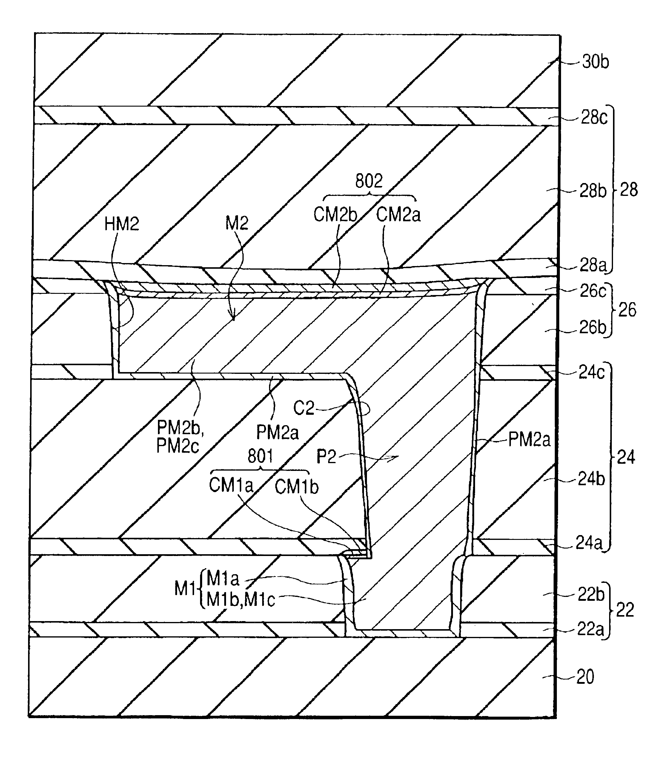
[0083]A semiconductor device according to the first embodiment of the present invention will be described in the order of its fabrication steps. FIGS. 1 to 23 are fragmentary cross-sectional or fragmentary plane views of a substrate illustrating the manufacturing method for production of a semiconductor device according to Embodiment 1 of the present invention.

[0084]As illustrated in FIG. 1, an n channel type MISFET (Metal Insulator Semiconductor Field Effect Transistor) Qn is formed over the main surface of a semiconductor substrate as one example of a semiconductor element.

[0085]The following is one example of an MISFET formation process.

[0086]First, a semiconductor substrate 1, a so-called SOI (silicon on Insulator) substrate, is prepared, which substrate has an insulating film, for example, a silicon oxide film 1b, formed over a semiconductor region 1a, and, further, a p type semiconductor region 1c is formed over the insulating film. Each element formation region ...

embodiment 2

(Embodiment 2)

[0165]In this Embodiment, an example of the laminated structure of an insulating film, in which a wiring trench and a contact hole are to be formed, will be described.

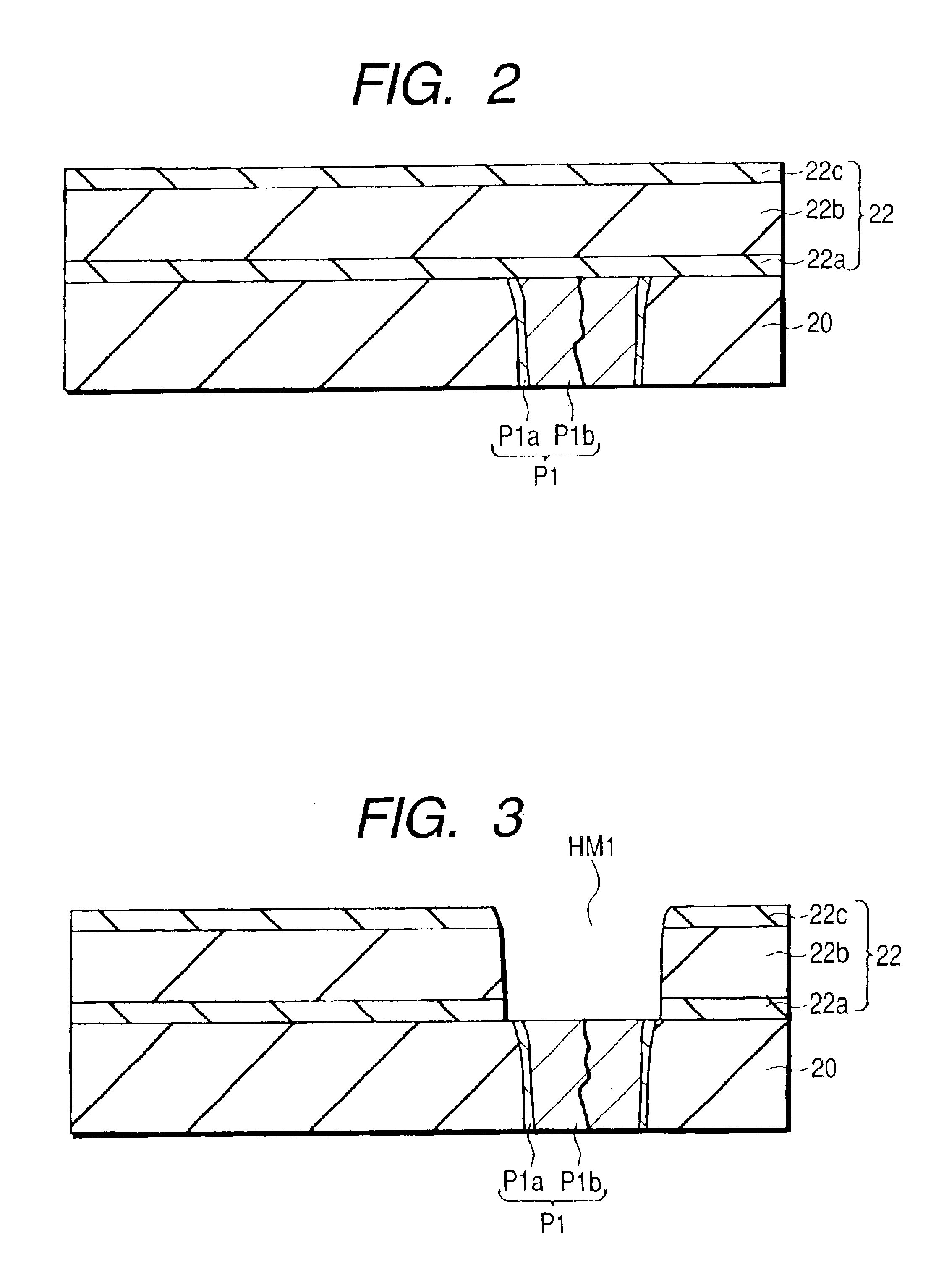
[0166](1) In Embodiment 1, the wiring trench HM2 and contact hole C2 were formed in a five-layer insulating film (24a, 24b, 24c, 26b, 26c) (refer to FIG. 12), but of these films, film 24a may be omitted. FIG. 24 is a fragmentary cross-sectional view of a substrate illustrating the manufacturing method for fabrication of a semiconductor device according to Embodiment 2 of the present invention.

[0167]The semiconductor device of this Embodiment of the present invention will be described in accordance with its manufacturing method. The steps up to the formation of the first-level interconnect M1 and the tungsten film CM1 thereover are similar to those of Embodiment 1, which steps were described with reference to FIGS. 1 to 6, so that the description of them will be omitted.

[0168]Then, as illustrated in FIG. 2...

embodiment 3

(Embodiment 3)

[0196]In Embodiment 1, the wiring trench HM2 to embed the second-level interconnect M2 therein was formed in the insulating film 26 and TEOS film 24c. This wiring trench HM2 may be formed in the insulating film 26. FIG. 26 is a fragmentary cross-sectional view of a substrate illustrating the manufacturing method for production of a semiconductor device according to Embodiment 3 of the present invention.

[0197]The semiconductor device of this embodiment of the present invention will be described in accordance with its manufacturing method. Steps up to the formation of the first-level interconnect M1 and the tungsten film CM1 thereover are similar to those described above for Embodiment 1 with reference to FIGS. 1 to 6, so that their description is omitted.

[0198]As illustrated in FIG. 26, a TEOS film 24a, an SiOC film 24b and another TEOS film 24c are successively deposited by CVD as an insulating film over the TEOS film 22c and tungsten film CM1. Then, over the TEOS film...


PUM


Abstract

A semiconductor device has first interlayer insulating film having a wiring trench; a wiring portion having a first barrier metal layer formed over side walls and bottom surface of the wiring trench, a first conductor layer formed over the first barrier metal layer to embed the wiring trench, and a capping barrier metal film formed over the first conductor layer; second interlayer insulating film formed over the first interlayer insulating film and having a connecting hole; and a connecting portion having a second barrier metal layer formed over side walls and bottom surface of the connecting hole, and a second conductor layer formed over the second barrier metal layer to embed the connecting hole; wherein, at a joint between the connecting portion and wiring portion, at least one of the second barrier metal layer and capping barrier metal film on the bottom surface of the connecting hole is removed.

Description

[0001]This is a continuation of application Ser. No. 10 / 294,937, filed Nov. 15, 2002, the entire disclosure of which is hereby incorporated by reference.BACKGROUND OF THE INVENTION[0002]The present invention relates in general to semiconductor integrated circuit devices; and, more particularly, the invention relates to a technique that is effective when applied to a connecting portion between interconnects in a semiconductor integrated circuit device.[0003]In recent years, in view of the tendency toward miniaturization and multi-layering of the interconnects of semiconductor integrated circuit devices (semiconductor devices), studies have been made of the so-called damascene technique for forming a trench in an insulating film and embedding it with a conductive film, thereby forming an interconnect.[0004]This damascene technology can be roughly divided into the single damascene technique and the dual damascene technique. In the former one, a wiring trench and a trench for connecting...

Claims


Application Information

Patent Timeline
Patent Type & Authority Patents(United States)
IPC IPC(8): H01L21/285H01L23/52H01L21/02H01L21/70H01L21/768H01L23/532H01L21/84H01L27/12H01L29/43H01L21/3205H01L29/423H01L29/49
CPCH01L21/28562H01L21/76801H01L21/76811H01L21/76814H01L21/76834H01L21/76835H01L21/76838H01L21/76844H01L21/76849H01L21/76877H01L21/84H01L23/53223H01L23/53238H01L23/53252H01L23/5329H01L27/1203H01L2924/0002H01L2924/00H01L21/3205
Inventor SAITO, TATSUYUKIOHASHI, NAOFUMIIMAI, TOSHINORINOGUCHI, JUNJITAMARU, TSUYOSHI
Owner RENESAS ELECTRONICS CORP
Why Eureka
Try Eureka