Semiconductor device and semiconductor device manufacturing method

a semiconductor device and semiconductor technology, applied in the direction of semiconductor devices, electrical equipment, transistors, etc., can solve the problems of increased manufacturing cost, increased leak current, and high cost of light ion irradiation devices, so as to achieve low cost and local control of carrier life, the effect of not increasing leak current or contaminating the manufacturing lin

Active Publication Date: 2015-10-29
FUJI ELECTRIC CO LTD
View PDF17 Cites 42 Cited by
  • Summary
  • Abstract
  • Description
  • Claims
  • Application Information

AI Technical Summary

Benefits of technology

[0022]According to the above mentioned invention, the defects are formed throughout the semiconductor substrate by electron beam irradiation, and then the defects on the substrate rear surface side are locally recovered by the hydrogen ion implantation from the substrate rear surface, whereby the carrier lifetime on the substrate rear surface side can be made longer than the carrier lifeline on the substra

Problems solved by technology

There is a method for obtaining the above mentioned predetermined carrier lifetime distribution by selectively irradiating such light ions as helium (He) and protons onto the anode side of the n−-type drift layer and decreasing the lifetime of the carriers in a portion where the light ions are irradiated, but in this case, the light ion irradiation device itself is expensive, which increases the manufacturing cost, and leak current may increase.
It is also possib

Method used


Image

  • Semiconductor device and semiconductor device manufacturing method
  • Semiconductor device and semiconductor device manufacturing method
  • Semiconductor device and semiconductor device manufacturing method

Examples


embodiment 1

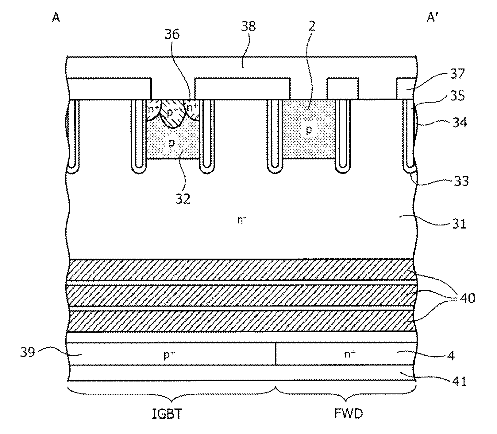
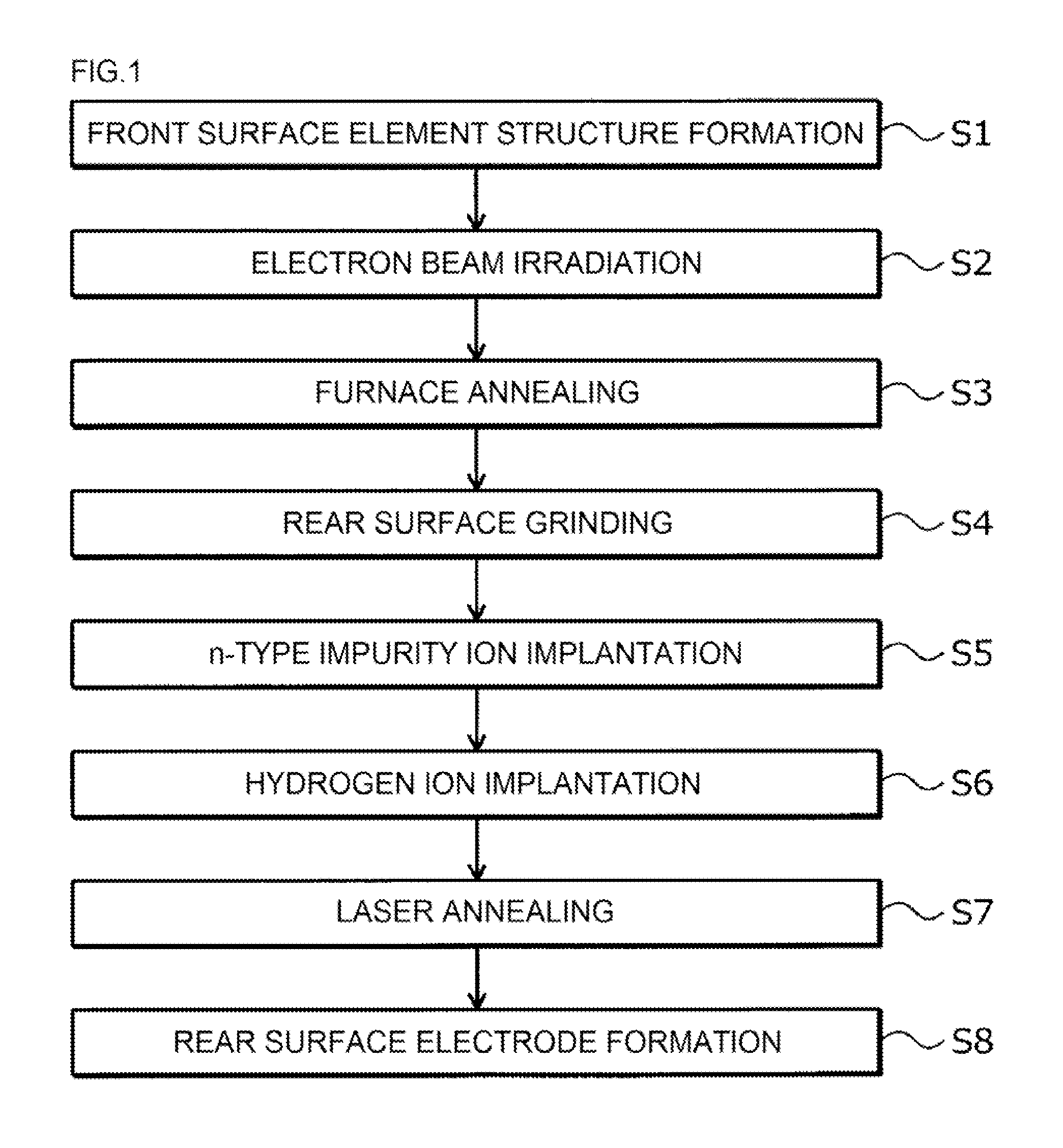
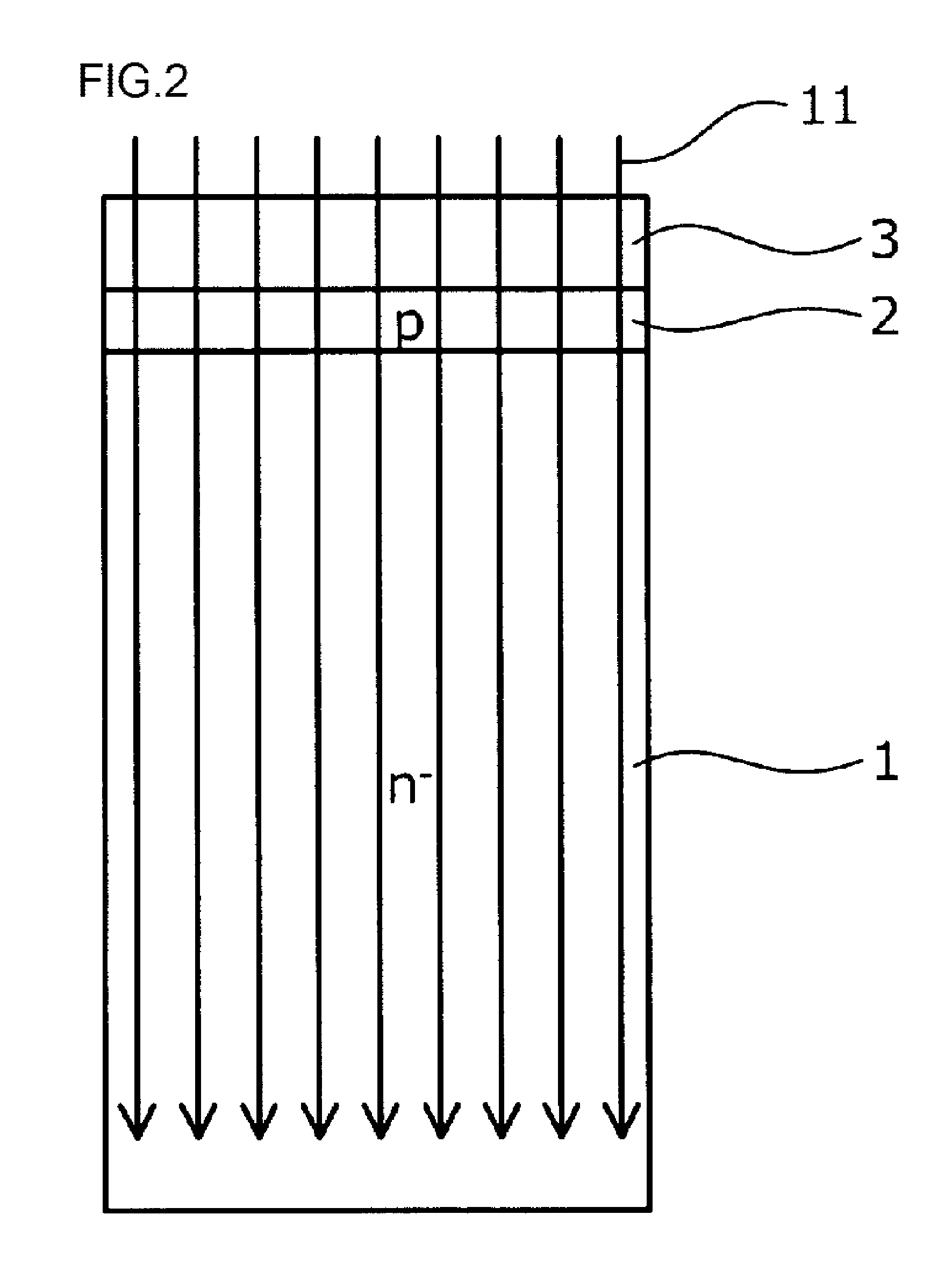
[0065]A semiconductor device manufacturing method according to Embodiment 1 will be described using an example of fabricating (manufacturing) a pin diode. FIG. 1 is a flow chart depicting an overview of the semiconductor device manufacturing method according to Embodiment 1. FIG. 2 to FIG. 7 are cross-sectional views depicting a state during manufacturing the semiconductor according to Embodiment 1. FIG. 8A and FIG. 8B are characteristic diagrams depicting an impurity concentration distribution of the semiconductor device according to Embodiment 1. First, a front surface element structure constituted by a p-type anode layer 2, an anode electrode 3, a terminal withstand voltage structure (not illustrated), and a passivation film (not illustrated) is formed on the front surface side of an n-type semiconductor substrate to be an n−-type drift layer 1 (step S1). In concrete terms, a p-type layer to be a p-type anode layer 2 and a p-type layer to be a guard ring constituting the terminal...

embodiment 2

[0081]A semiconductor device manufacturing method according to Embodiment 2 will be described using an example of fabricating a pin diode, which includes an n-type field stop (FS) layer constituted by a hydrogen inducing donor, inside the n−-type drift layer. FIG. 11 is a flow chart depicting an overview of the semiconductor device manufacturing method according to Embodiment 2. FIG. 12A and FIG. 12B are characteristic diagrams depicting an impurity concentration distribution of the semiconductor device according to Embodiment 2. A difference of the semiconductor device manufacturing method according to Embodiment 2 from the semiconductor device manufacturing method according to Embodiment 1 is that the implantation depth of the hydrogen ion implantation from the substrate rear surface is made deeper than the penetration depth of the laser from the substrate rear surface in the laser annealing for activating the n+-type cathode layer 4.

[0082]First, a front surface element structure ...

embodiment 3

[0090]A semiconductor device manufacturing method according to Embodiment 3 will be described next. FIG. 13 is a flow chart depicting an overview of the semiconductor device manufacturing method according to Embodiment 3. A difference of the semiconductor device manufacturing method according to Embodiment 3 from the semiconductor device manufacturing method according to Embodiment 1 is that the electron beam irradiation and the furnace annealing are performed after the laser annealing. The semiconductor device manufacturing method according to Embodiment 3 is useful when defects are formed in a shallow region, such as 3 μm or less from the substrate rear side, by the hydrogen ion implantation (e.g. a case of fabricating a pin diode which does not include an FS layer).

[0091]In concrete terms, in the same manner as in Embodiment 1, the front surface element structure is formed (step S21). Then the rear surface grinding (step S22), the hydrogen ion implantation (step S23), the n-type ...


PUM


Abstract

A front surface element structure is formed on the front surface side of an n-type semiconductor substrate. Then defects are formed throughout an n-type semiconductor substrate to adjust a carrier lifetime. Hydrogen ions are ion-implanted from a rear surface side of the n-type semiconductor substrate, and a hydrogen implanted region having a hydrogen concentration higher than a hydrogen concentration of a bulk substrate is formed in the surface layer of a rear surface side of the n-type semiconductor substrate.

Description

CROSS-REFERENCE TO RELATED APPLICATIONS[0001]This application is a continuation under 35 U.S.C. 120 of International Application PCT / JP2014 / 066069 having the International Filing Date of Jun. 17, 2014, and having the benefit of the earlier filing date of Japanese Application No. 2013-134329, filed on Jun. 26, 2013. All of the identified applications are fully incorporated herein by reference.TECHNICAL FIELD[0002]The present invention relates to a semiconductor device and a semiconductor device manufacturing method.BACKGROUND ART[0003]As a semiconductor device used for power semiconductor devices, diodes and IGBTs (Insulated Gate Bipolar Transistor) having a withstand voltage of 400V, 600 V, 1200V, 1700V, 3300V or more are known. These diodes and IGBTs are used for power conversion devices, such as convertors and invertors, and are demanded to have low loss, low noise and high breakdown tolerance, as well as low cost. As an example of the semiconductor device used for power semicondu...

Claims


Application Information

Patent Timeline
IPC IPC(8): H01L29/06H01L29/739H01L21/324H01L21/268H01L21/26H01L29/861H01L21/265
CPCH01L29/0615H01L29/861H01L29/7397H01L21/324H01L21/268H01L21/2605H01L21/26513H01L21/263H01L29/0834H01L29/32H01L29/66136H01L29/66333H01L29/66348H01L29/868H01L29/36H01L21/26506
Inventor ONOZAWA, YUICHITAKISHITA, HIROSHIYOSHIMURA, TAKASHI
Owner FUJI ELECTRIC CO LTD
Why Eureka
Try Eureka