Fabrication method of semiconductor package structure

a technology of semiconductor package structure and fabrication method, which is applied in the direction of semiconductor device details, line/current collector details, semiconductor/solid-state device details, etc., can solve the problems of low reliability of solder joints, difficult control of gaps, and easy cracking of solder joints, so as to improve the electrical connection quality of the package structure, prevent tangling of bonding wires, and shorten bonding wires

Active Publication Date: 2012-11-06
SILICONWARE PRECISION IND CO LTD
View PDF20 Cites 5 Cited by
  • Summary
  • Abstract
  • Description
  • Claims
  • Application Information

AI Technical Summary

Benefits of technology

[0019]In addition, the contact pad areas are arranged in array to surround the die mounting area, and the bond pads are disposed at the periphery of the die pad, thereby shortening the bonding wires electrically connecting the semiconductor chip and the bond pads.
[0021]According to the present invention, the bond pads and traces formed at the chip mounting side of the dielectric layer shorten the bonding wires and prevent tangling of the bonding wires, thereby improving the electrical connection quality of the package structure. Further, when the semiconductor package structure is soldered to a circuit board, since the metal pillars protrude from the bottom surface of the dielectric layer, it facilitates the formation of stable solder joints between the metal pillars and the circuit board and prevents solder overflow and bridging. In addition, the present invention provides high density and array arranged I / O connections so as to extend the application range of the semiconductor package structure.

Problems solved by technology

However, since the contact pads are closely arranged and do not protrude from the bottom surface of the semiconductor package structure 1, when the semiconductor package structure 1 is soldered to the circuit board 15, the gap between the contact pads 101 and the solder pads 151 of the circuit board 15 is so small that it is difficult to control the gap.
As a result, the reliability of the solder joints is low, the solder joints are easy to crack, and the soldering situation is difficult to check.
Further, the semiconductor package structure 1 cannot provide array arranged contact pads and accordingly cannot provide a semiconductor package structure with high density I / O connections.
However, although a certain gap is provided between the contact pads and the circuit board and array-arranged contact pads are provided, since long bonding wires are required to electrically connect the semiconductor chip to the contact pads located far away, it adversely affects the electrical performance of the package structure.
Further, due to tangling of the bonding wires, it is difficult for the package structure to provide high density I / O connections.

Method used


Image

  • Fabrication method of semiconductor package structure
  • Fabrication method of semiconductor package structure
  • Fabrication method of semiconductor package structure

Examples


Embodiment Construction

[0027]The following illustrative embodiments are provided to illustrate the disclosure of the present invention, these and other advantages and effects can be apparent to those in the art after reading this specification.

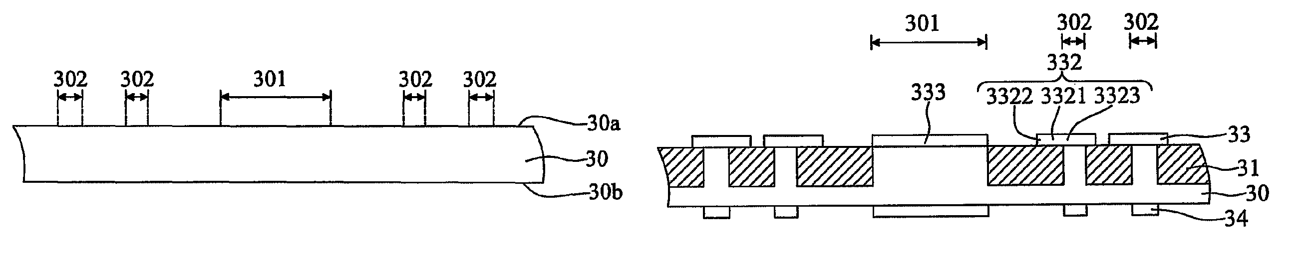
[0028]FIGS. 3A to 3G are cross-sectional views showing a fabrication method of a semiconductor package structure according to a preferred embodiment of the present invention, wherein FIG. 3E′ is a top view, and FIG. 3E is a cross-sectional view taken along line 3E-3E of FIG. 3E′.

[0029]Referring to FIG. 3A, a metal plate 30 having a first surface 30a and an opposite second surface 30b is provided, wherein the first surface 30a has a die mounting area 301 and a plurality of contact pad areas 302. The metal plate 30 can be made of copper.

[0030]Referring to FIG. 3B, the metal plate 30 is patterned from the first surface 30a towards the second surface 30b so as to form a plurality of concave portions 300 in the metal plate 30 outside the die mounting area 301 and the con...


PUM

PropertyMeasurementUnit
areaaaaaaaaaaa
areasaaaaaaaaaa
dielectricaaaaaaaaaa

Abstract

A fabrication method of a semiconductor package structure includes: patterning a metal plate having first and second surfaces; forming a dielectric layer on the metal plate; forming a metal layer on the first surface and the dielectric layer; forming metal pads on the second surface, the metal layer having a die pad and traces each having a bond pad; mounting a semiconductor chip on the die pad, followed by connecting electrically the semiconductor chip to the bond pads through bonding wires; forming an encapsulant to cover the semiconductor chip and the metal layer; removing portions of the metal plate not covered by the metal pads so as to form metal pillars; and performing a singulation process. The fabrication method is characterized by disposing traces with bond pads close to the die pad to shorten the bonding wires and forming metal pillars protruding from the dielectric layer to avoid solder bridging.

Description

CROSS-REFERENCES TO RELATED APPLICATIONS[0001]This application claims under 35 U.S.C. §119(a) the benefit of Taiwanese Application No. 098146227 filed Dec. 31, 2009 the entire contents of which is incorporated herein by reference.BACKGROUND OF THE INVENTION[0002]1. Field of the Invention[0003]The present invention relates to fabrication methods of semiconductor package structures, and more particularly, to a fabrication method of a semiconductor package structure characterized by high quality of wire bonding but not susceptible to solder bridging.[0004]2. Description of Related Art[0005]In a conventional lead frame based semiconductor package such as a QFN (Quad Flat Non-lead) package, a semiconductor chip is attached and wire-bonded to a lead frame and encapsulated by an encapsulant, and metal portions around the lead frame are exposed from the encapsulant to serve as contact pads for connection with an external device. A semiconductor package structure thus fabricated is advantage...

Claims


Application Information

Patent Timeline
Patent Type & Authority Patents(United States)
IPC IPC(8): H01L21/44
CPCH01L21/4832H01L23/4951H01L23/3107H01L23/495Y10T29/49171H01L2224/48091H01L2224/48247H01L2224/49171H01L2924/01046H01L2924/01079Y10T29/49117Y10T29/49172H01L24/49H01L24/48H01L2924/00014H01L2924/00H01L2924/181H01L2924/00012H01L2224/45099H01L2224/45015H01L2924/207
Inventor LIN, PANG-CHUNLI, CHUN-YUANHUANG, CHIEN-PINGKE, CHUN-CHI
Owner SILICONWARE PRECISION IND CO LTD
Why Eureka
Try Eureka