Non-volatile latch circuit and logic circuit, and semiconductor device using the same

a logic circuit and latch circuit technology, applied in pulse generators, pulse techniques, instruments, etc., can solve problems such as increased variation, low hydrogen concentration, and reduced voltage reliability, and achieve low carrier concentration, high purification, and low cost

Active Publication Date: 2012-11-20
SEMICON ENERGY LAB CO LTD
View PDF136 Cites 83 Cited by
  • Summary
  • Abstract
  • Description
  • Claims
  • Application Information

AI Technical Summary

Benefits of technology

[0006]One embodiment of the present invention is a latch circuit with a loop structure, in which an output of a first element is electrically connected to an input of a second element and an output of the second element is electrically connected to an input of the first element through a second transistor. A transistor using an oxide semiconductor as a semiconductor material of a channel formation region is used as a switching element, and a capacitor is provided to be electrically connected to a source electrode or a drain electrode of the transistor, whereby data of the latch circuit can be retained, and a non-volatile latch circuit can thus be formed. The transistor using an oxide semiconductor allows retaining data written to the capacitor. The capacitor is electrically connected to a predetermined position in the loop structure of the latch circuit. Accordingly, the non-volatile latch circuit has such a configuration that a charge corresponding to data of the latch circuit is automatically accumulated in the capacitor so that data writing is performed.
[0020]Accordingly, when the transistor using an oxide semiconductor layer for a channel formation region is used as a switching element, a charge accumulated in the capacitor can be kept retained even after the supply of a power source voltage to the latch circuit has stopped. That is, data written to the capacitor can be kept retained.
[0021]For example, it is possible to realize a much longer refresh time than that of a DRAM which is formed using a transistor including a channel formation region made of silicon, and also to realize memory retention characteristics (data retaining characteristics) almost as good as those of a non-volatile memory. Furthermore, after a power source voltage has restarted to be supplied to the latch circuit, data retained in the capacitor can be read. As a result, the logic state can be returned to that before the supply of a power source voltage stops.
[0026]As described above, in one embodiment of the present invention, the transistor using an oxide semiconductor as a semiconductor material of a channel formation region is used as the switching element; thus, it is possible to provide a non-volatile latch circuit which operates in a wide temperature range and stably operates even at high temperature, and in which a stored logic state is not erased even when the power is turned off.
[0036]According to one embodiment of the present invention, a transistor using, as a semiconductor material of a channel formation region, an intrinsic (i-type) or substantially intrinsic (i-type) oxide semiconductor which has a sufficiently low hydrogen concentration to be highly purified and to have a sufficiently low carrier concentration, is used as a switching element and a capacitor electrically connected to a source electrode or a drain electrode of the transistor is provided; thus, it is possible to realize a non-volatile latch circuit which operates in a wide temperature range and stably operates even at high temperature, and in which a stored logic state is not erased even when the power is turned off, or a latch circuit which has a sufficiently long refresh time and data retention characteristics. In addition, since a charge accumulated in the capacitor is retained as data, data can be read easily with less variation as compared with the case where data is stored by remanent polarization.
[0037]Various kinds of logic circuits can be provided by using the non-volatile latch circuit. For example, the power consumption of a logic circuit using the non-volatile latch circuit can be reduced by turning off the power of blocks not in use. In addition, since a logic state is stored even when the power is turned off, a system can be started when the power is turned on or terminated when the power is turned off, at high speed and low power.

Problems solved by technology

However, a non-volatile latch circuit using a ferroelectric element has problems with reliability of the number of rewrites and reduction in voltage.
However, when the remanent polarization is small, the influence of variation increases or a high-accuracy reading circuit is needed.

Method used


Image

  • Non-volatile latch circuit and logic circuit, and semiconductor device using the same
  • Non-volatile latch circuit and logic circuit, and semiconductor device using the same
  • Non-volatile latch circuit and logic circuit, and semiconductor device using the same

Examples


embodiment 1

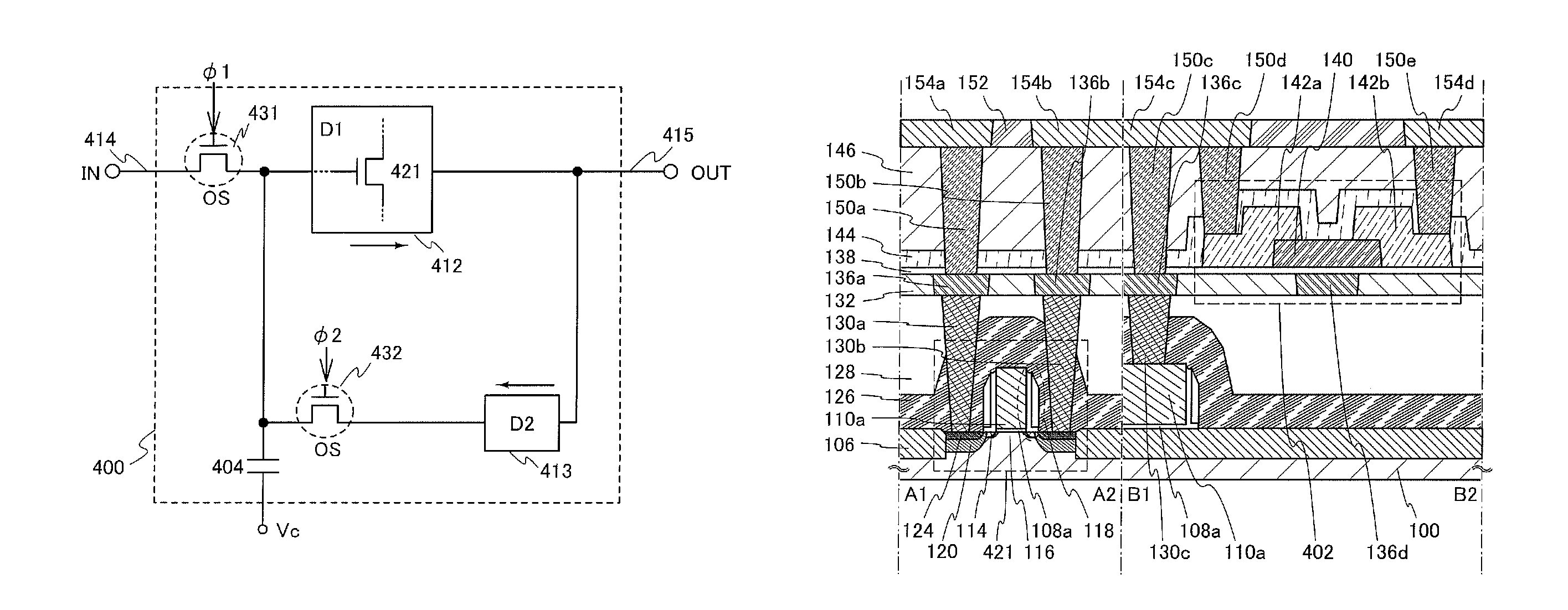
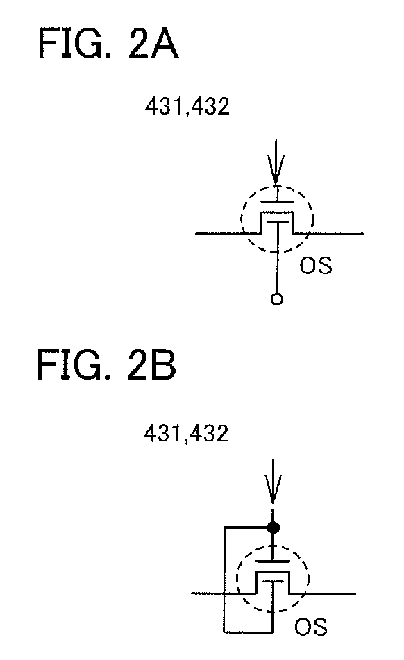
[0061]In this embodiment, a configuration and operation of a non-volatile latch circuit which is one embodiment of the disclosed invention, a configuration and a method for manufacturing an element included in the non-volatile latch circuit, and the like will be described with reference to FIG. 1, FIGS. 2A and 2B, FIGS. 3A and 3B, FIGS. 4A to 4H, FIGS. 5A to 5G, FIGS. 6A to 6D, FIG. 7, FIG. 8, FIGS. 9A and 9B, and FIG. 10.

[0062]FIG. 1 illustrates a configuration of a non-volatile latch circuit 400. The non-volatile latch circuit 400 illustrated in FIG. 1 has a loop structure in which an output of a first element (D1) 412 is electrically connected to an input of a second element (D2) 413 and an output of the second element (D2) 413 is electrically connected to an input of the first element (D1) 412 through a second transistor 432.

[0063]The input of the first element (D1) 412 is electrically connected to a wiring 414 to which an input signal is applied through a first transistor 431. ...

embodiment 2

[0233]In this embodiment, a configuration and operation of the non-volatile latch circuit that is an embodiment of the disclosed invention will be described with reference to FIGS. 11A and 11B and FIG. 12.

[0234]FIG. 11A illustrates a configuration of the non-volatile latch circuit 400. FIG. 11B illustrates a configuration of part of the non-volatile latch circuit 400. FIG. 12 is an example of a timing chart of the non-volatile latch circuit 400.

[0235]FIG. 11A illustrates an example of the configuration of the latch circuit 400 in FIG. 1, where a first inverter is used as the first element 412 and a second inverter is used as the second element 413. The first transistor 431 and the second transistor 432 can have a structure similar to that shown in Embodiment 1. That is, as the first transistor 431 and the second transistor 432, it is possible to use a transistor which uses an oxide semiconductor layer for a channel formation region and has normally-off characteristics and a signific...

embodiment 3

[0257]In this embodiment, operation of the non-volatile latch circuit that is an embodiment of the disclosed invention will be described with reference to FIGS. 13A and 13B. The non-volatile latch circuit has the same configuration as that illustrated in FIGS. 11A and 11B, and the timing chart thereof is different from that of FIG. 12.

[0258]FIG. 13A illustrates an example of a timing chart of potentials of a signal φ1, a signal φ2, an input signal IN, and an output signal OUT obtained during a period when the non-volatile latch circuit 400 operates (operation period) and a period when the non-volatile latch circuit 400 does not operate (non-operation period). FIG. 13A also illustrates a potential of the node S in the latch circuit 400, a potential of the power source voltage VDD applied to the first element (first inverter) 412 and the second element (second inverter) 413, and a potential Vc of the other electrode of the capacitor 404.

[0259]In FIG. 13A, a period a, a period b, a per...


PUM


Abstract

A novel non-volatile latch circuit and a semiconductor device using the non-volatile latch circuit are provided. The latch circuit has a loop structure in which an output of a first element is electrically connected to an input of a second element and an output of the second element is electrically connected to an input of the first element through a second transistor. A transistor using an oxide semiconductor as a semiconductor material of a channel formation region is used as a switching element, and a capacitor is provided to be electrically connected to a source electrode or a drain electrode of the transistor, whereby data of the latch circuit can be retained, and a non-volatile latch circuit can thus be formed.

Description

TECHNICAL FIELD[0001]The disclosed invention relates to a non-volatile logic circuit in which a stored logic state is not erased even when the power is turned off, and a semiconductor device using the non-volatile logic circuit. In particular, the disclosed invention relates to a non-volatile latch circuit and a semiconductor device using the same.BACKGROUND ART[0002]An integrated circuit including a non-volatile logic circuit has been proposed; in the integrated circuit, a logic circuit has “non-volatile” characteristics, i.e., memory of the logic circuit is not erased even when the power is turned off. For example, a non-volatile latch circuit using a ferroelectric element as a non-volatile logic circuit is proposed (Patent Document 1).REFERENCE[0003][Patent Document 1] PCT International Publication No. 2003 / 044953DISCLOSURE OF INVENTION[0004]However, a non-volatile latch circuit using a ferroelectric element has problems with reliability of the number of rewrites and reduction in...

Claims


Application Information

Patent Timeline
Patent Type & Authority Patents(United States)
IPC IPC(8): H01L25/00H03K19/00
CPCG11C14/0063H01L21/8258H01L27/0688H01L27/088H01L27/1225H01L27/1203H03K3/356008H03K3/35606H03K19/1733H01L21/84H01L29/7869G11C16/02H01L27/1156H10B41/70H01L27/1255
Inventor KATO, KIYOSHIKOYAMA, JUN
Owner SEMICON ENERGY LAB CO LTD
Why Eureka
Try Eureka