Semiconductor Device

a technology of semiconductor layer and semiconductor layer, which is applied in the direction of semiconductor layer, electrical apparatus, transistor, etc., can solve the problems of negative threshold voltage shift, insufficient oxygen supply of oxide semiconductor layer, etc., and achieve high on-state current, high integration, and favorable electric characteristics

Active Publication Date: 2015-07-30
SEMICON ENERGY LAB CO LTD
View PDF12 Cites 20 Cited by
  • Summary
  • Abstract
  • Description
  • Claims
  • Application Information

AI Technical Summary

Benefits of technology

[0032]In one embodiment of the present invention, any of the following semiconductor devices can be provided: a semiconductor device with favorable electric characteristics, a semiconductor device that is suitable for miniaturization, a semiconductor device with ...

Problems solved by technology

However, when the source and drain electrode layers are in contact with the oxide insulating layer, which is used as a base insulating film, over a large area, a problem arises in that oxygen in the oxide insulating layer cannot be sufficiently supplied to the oxid...

Method used


Image

  • Semiconductor Device
  • Semiconductor Device
  • Semiconductor Device

Examples


embodiment 1

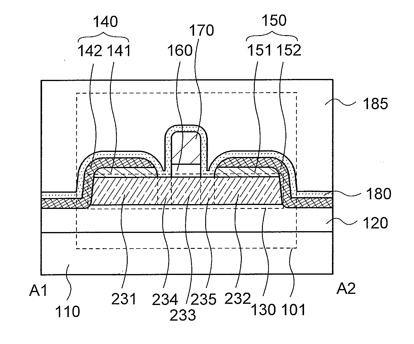
[0091]In this embodiment, transistors of one embodiment of the present invention will be described with reference to drawings.

[0092]In a transistor of one embodiment of the present invention, silicon (including strained silicon), germanium, silicon germanium, silicon carbide, gallium arsenide, aluminum gallium arsenide, indium phosphide, gallium nitride, an organic semiconductor, an oxide semiconductor, or the like can be used for a channel formation region. It is particularly preferable to use an oxide semiconductor having a wider band gap than silicon for the channel formation region.

[0093]For example, the oxide semiconductor preferably contains at least indium (In) or zinc (Zn). Further preferably, the oxide semiconductor contains an oxide represented by an In-M-Zn-based oxide (M is a metal such as Al, Ti, Ga, Ge, Y, Zr, Sn, La, Ce, or Hf).

[0094]In the description below, unless otherwise specified, a transistor described as an example includes an oxide semiconductor in a channel ...

embodiment 2

[0146]In this embodiment, transistors each having a structure different from the structures described in Embodiment 1 will be described with reference to drawings. Note that descriptions of components, effects, and the like which overlap with those in Embodiment 1 are omitted.

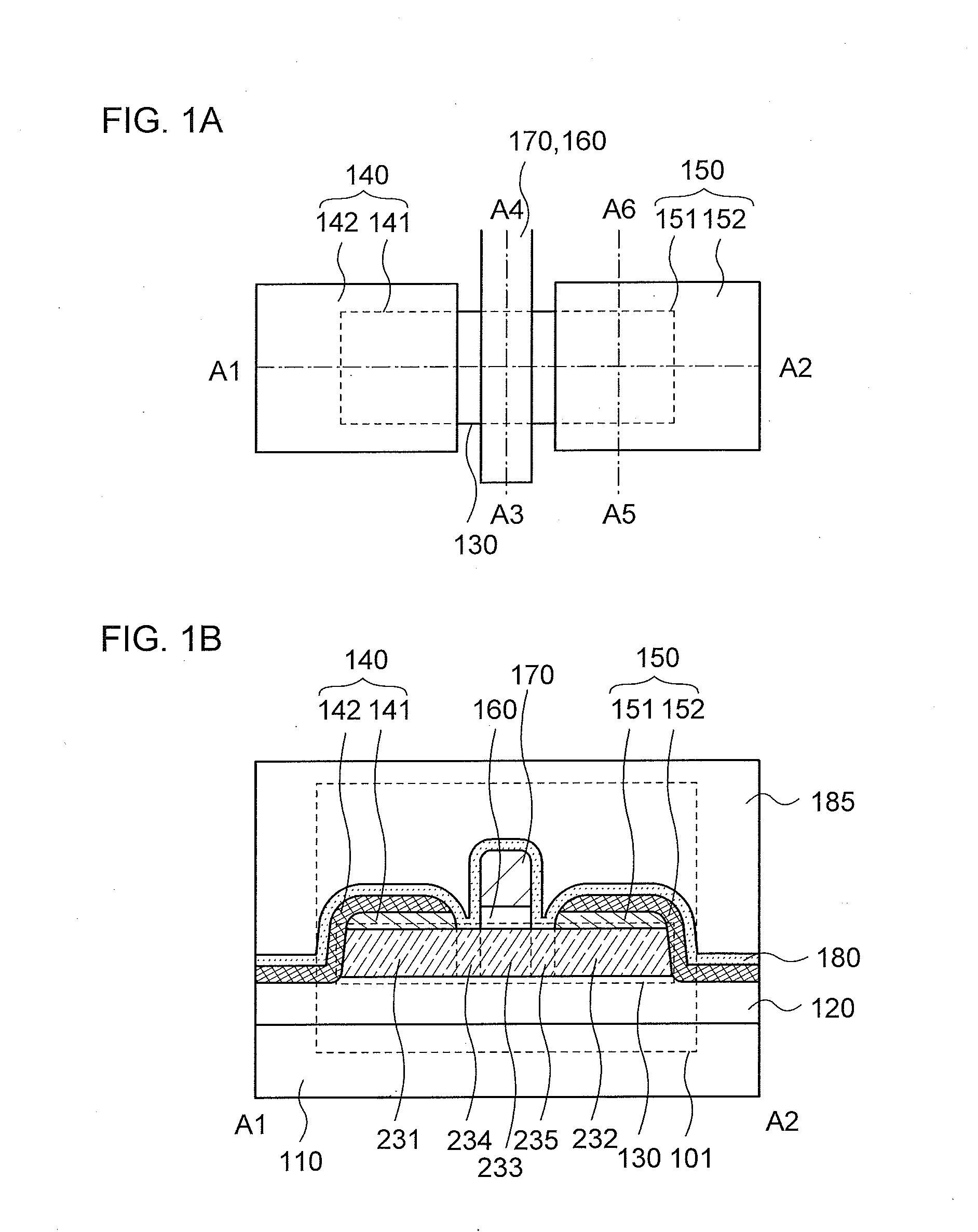
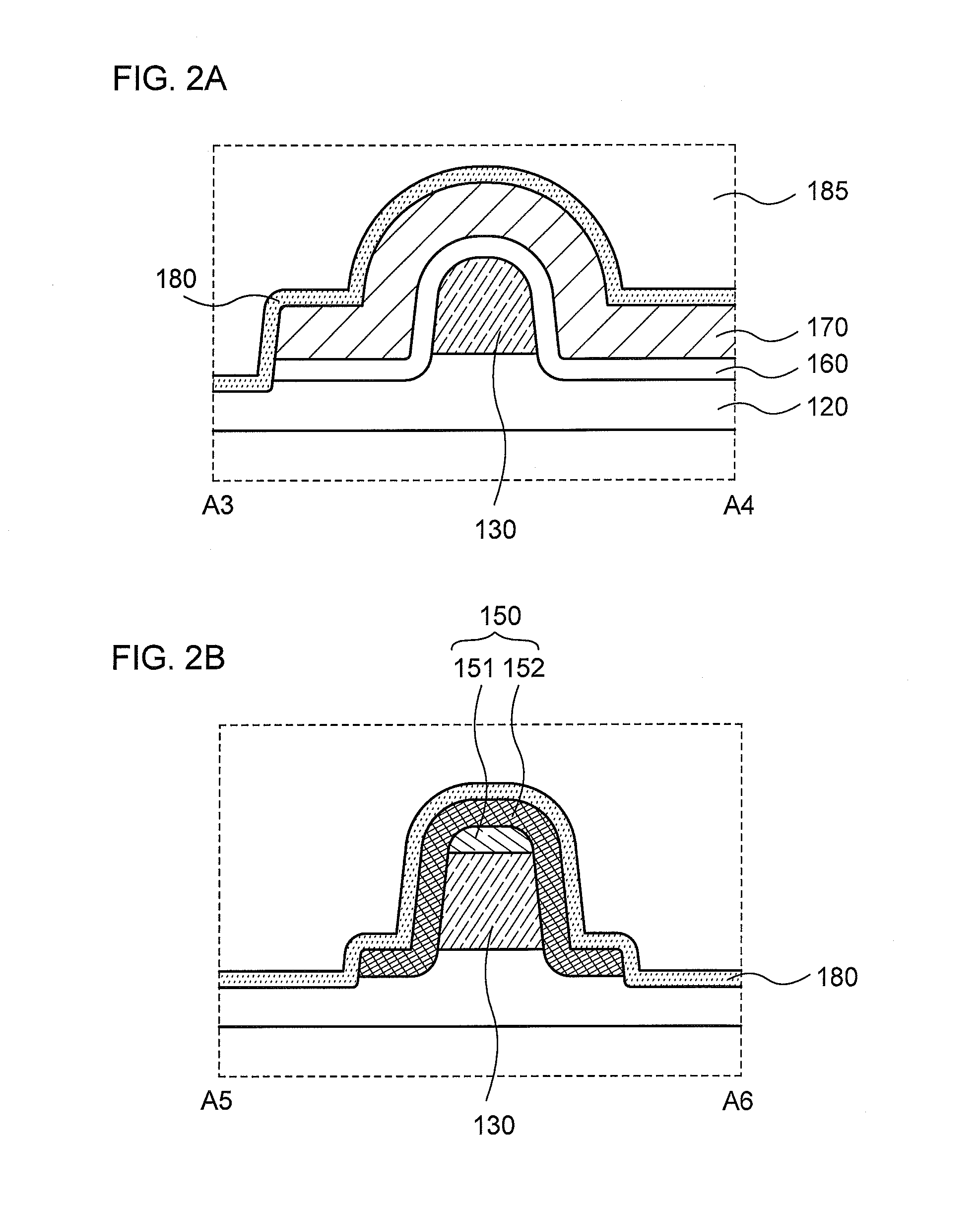
[0147]FIGS. 13A and 13B are a top view and a cross-sectional view of a transistor 104 of one embodiment of the present invention. FIG. 13A is the top view. FIG. 13B illustrates a cross section in the direction of a dashed-dotted line D1-D2 in FIG. 13A. Note that cross sections in the directions of the dashed-dotted lines D3-D4 and D5-D6 in FIG. 13A are the same as the cross sections of the transistor 101 in the directions of the dashed-dotted lines A3-A4 and A5-A6, which are illustrated in FIGS. 2A and 2B. In FIGS. 13A and 13B, some components are enlarged, reduced in size, or omitted for simplification. In some cases, the direction of the dashed-dotted line D1-D2 is referred to as a channel length direction, a...

embodiment 3

[0174]In this embodiment, components of the transistors described in Embodiment 1 will be described in detail.

[0175]The substrate 110 is not limited to a simple supporting substrate, and may be a substrate where another device such as a transistor is formed. In that case, at least one of the gate electrode layer 170, the source electrode layer 140, and the drain electrode layer of the transistor may be electrically connected to the above device.

[0176]For the substrate 110, for example, a glass substrate, a ceramic substrate, a quartz substrate, a sapphire substrate, or the like can be used. Alternatively, a single crystal semiconductor substrate or a polycrystalline semiconductor substrate of silicon or silicon carbide, a compound semiconductor substrate of silicon germanium, a silicon-on-insulator (SOI) substrate, or the like can be used.

[0177]The insulating layer 120 can have a function of supplying oxygen to the oxide semiconductor layer 130 as well as a function of preventing di...


PUM


Abstract

A semiconductor device having favorable electric characteristics is provided. An oxide semiconductor layer includes first and second regions apart from each other, a third region which is between the first and second regions and overlaps with a gate electrode layer with a gate insulating film provided therebetween, a fourth region between the first and third regions, and a fifth region between the second and third regions. A source electrode layer includes first and second conductive layers. A drain electrode layer includes third and fourth conductive layers. The first conductive layer is formed only over the first region. The second conductive layer is in contact with an insulating layer, the first conductive layer, and the first region. The third conductive layer is formed only over the second region. The fourth conductive layer is in contact with the insulating layer, the third conductive layer, and the second region.

Description

BACKGROUND OF THE INVENTION[0001]1. Field of the Invention[0002]One embodiment of the present invention relates to a semiconductor device including an oxide semiconductor, and a manufacturing method thereof.[0003]One embodiment of the present invention is not limited to the above technical field. The technical field of one embodiment of the invention disclosed in this specification and the like relates to an object, a method, or a manufacturing method. One embodiment of the present invention relates to a process, a machine, manufacture, or a composition of matter. Specifically, examples of the technical field of one embodiment of the present invention disclosed in this specification include a semiconductor device, a display device, a liquid crystal display device, a light-emitting device, a lighting device, a power storage device, a memory device, a method for driving any of them, and a method for manufacturing any of them.[0004]In this specification and the like, a semiconductor de...

Claims


Application Information

Patent Timeline
IPC IPC(8): H01L29/786
CPCH01L29/7869H01L29/78648H01L29/78696H01L29/78606
Inventor ITO, DAIGOHANAOKA, KAZUYA
Owner SEMICON ENERGY LAB CO LTD
Why Eureka
Try Eureka