Nonvolatile magnetic memory device

a magnetic memory and non-volatile technology, applied in semiconductor devices, digital storage, instruments, etc., can solve the problems of difficult microprocessing of ferroelectric material layers, lower than desired, and write speed on the order of microseconds, so as to improve the index of thermal stability in the equation (1), increase the coercive force hc, and improve the anisotropy field hk.

Active Publication Date: 2009-09-10
SONY CORP
View PDF0 Cites 18 Cited by
  • Summary
  • Abstract
  • Description
  • Claims
  • Application Information

AI Technical Summary

Benefits of technology

[0069]Since large tensile stress or compressive stress can be applied to the recording layer along the easy magnetization axis of the recording layer, the value of the third term [3(λ / Ms)·σ] of the right-handed side in the equation (2) can be increased. As a result, the coercive force Hc can be increased due to a Villari effect, also called an inverse magnetostriction effect, and thus the anisotropy field Hk can be increased. Therefore, the index Δ of thermal stability in the equation (1) can be improved. For this reason, it is possible to provide a nonvolatile magnetic memory device that includes a highly reliable magnetoresistance effect element capable of improving thermal stability of the recording layer and a data retaining characteristic. The magnitude of stress (σ) does not depend on the material forming the recording layer. As a result, by appropriately selecting of a material forming the recording layer, for example, a critical current (write current) Ic of spin-injection magnetization inversion can be reduced, and thus low power consumption of the nonvolatile magnetic memory device can be achieved.

Problems solved by technology

However, the flash memories have the defects that the write speed is on the order of microseconds, which is lower than desired.
Meanwhile, the FERAM has a number of times of rewriting possible on the order of 1012 to 1014, which is too low for the FERAM to be used in place of SRAM or DRAM, and micro-processing of the ferroelectric material layer is difficult to carry out.
However, with the miniaturization of the MRAM, the bit line BL is made finer, and accordingly a sufficient amount of current is difficult to pass through the bit line BL.

Method used


Image

  • Nonvolatile magnetic memory device
  • Nonvolatile magnetic memory device
  • Nonvolatile magnetic memory device

Examples


example 1

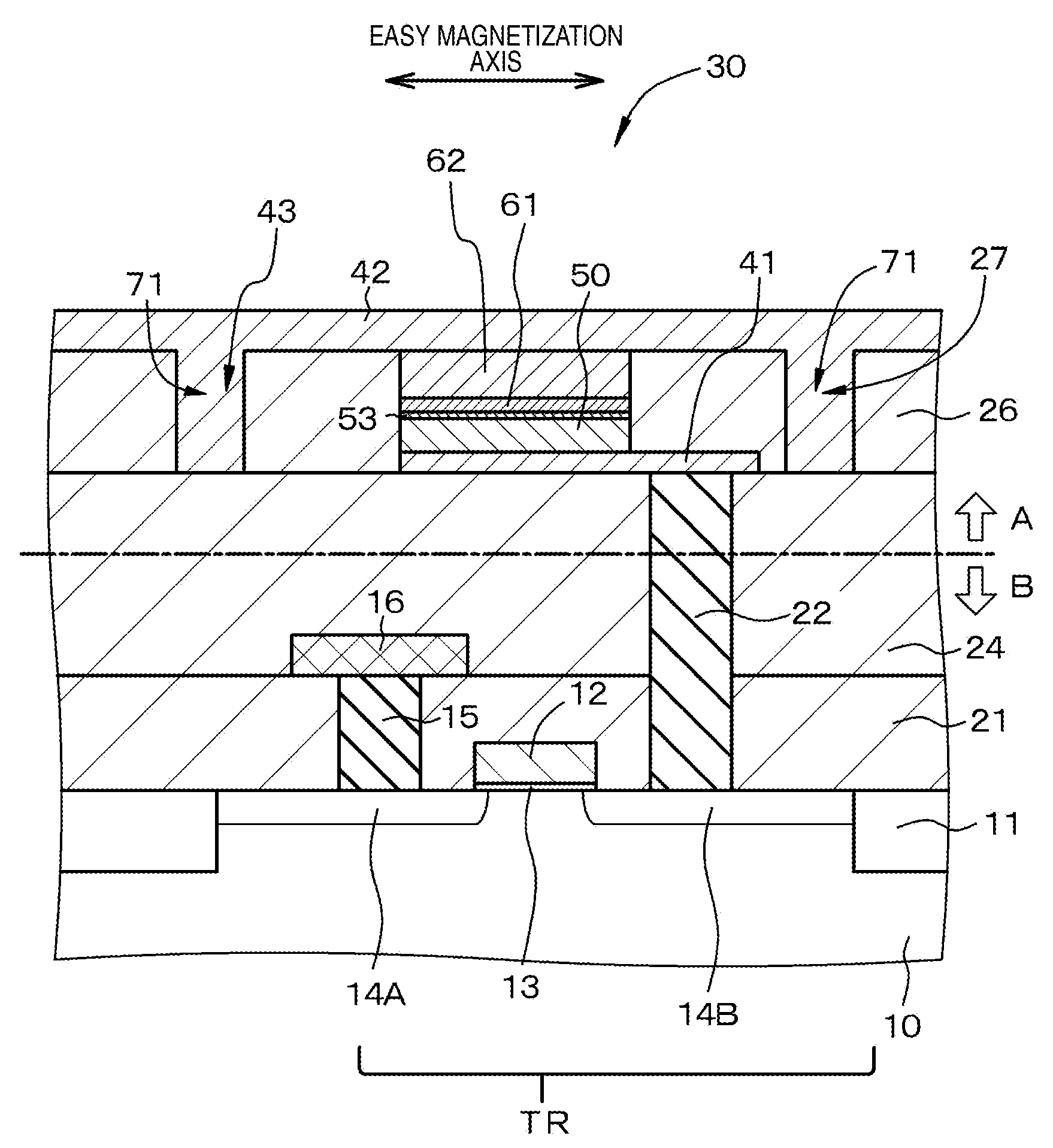
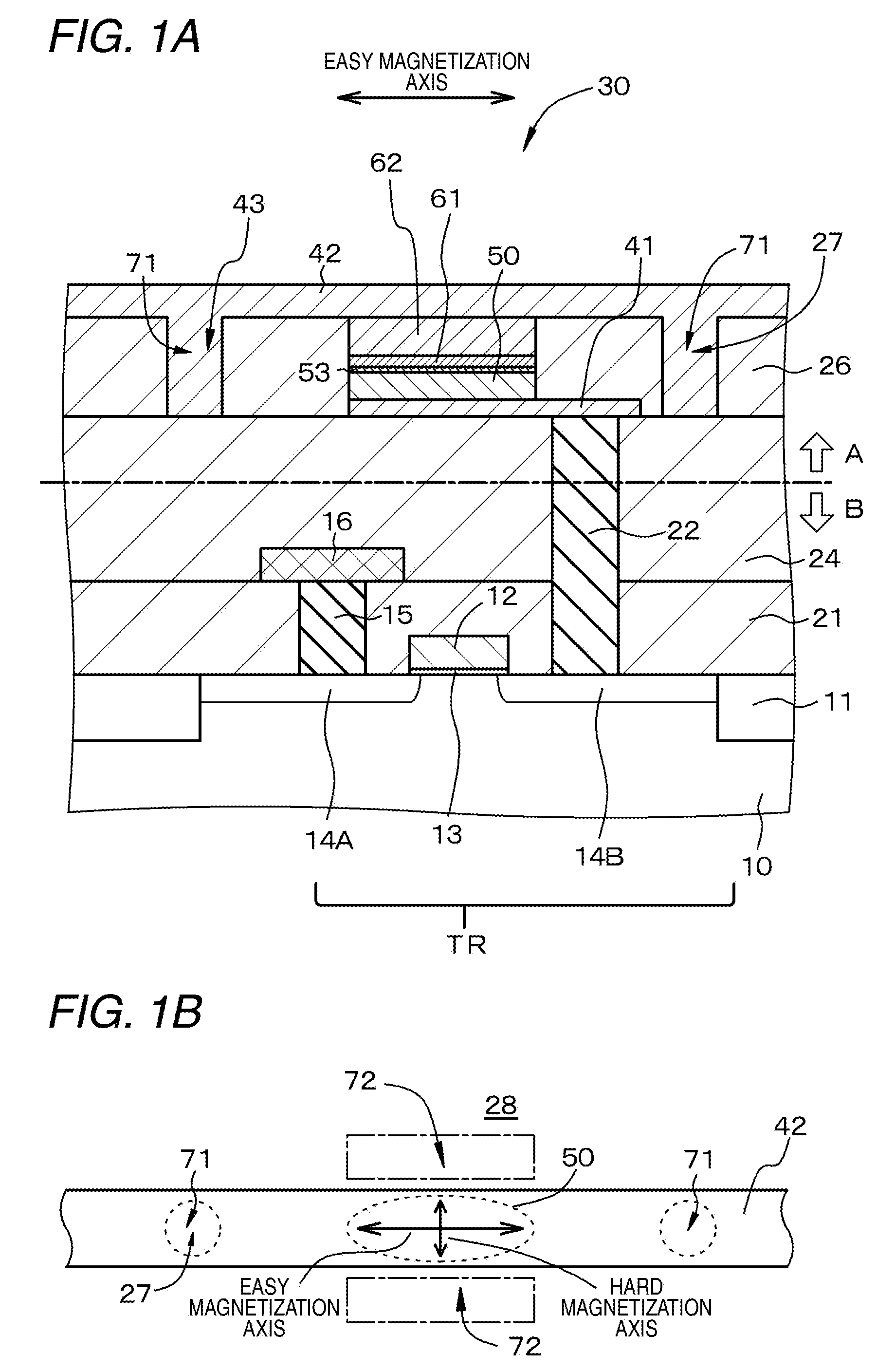
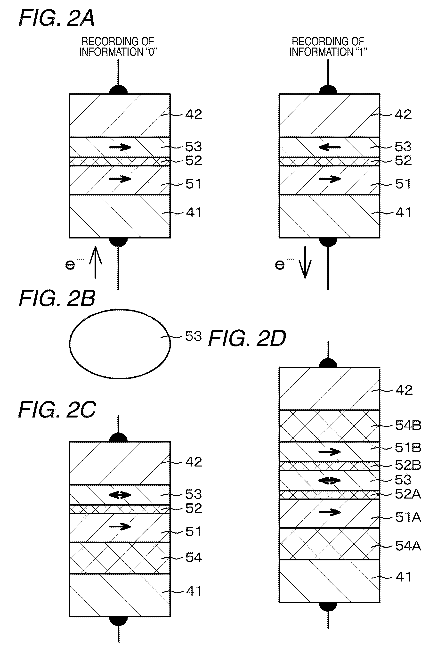
[0090]Example 1 relates to the nonvolatile magnetic memory device according to the first and third embodiments of the invention, and specifically, to first configuration. A schematic partial sectional view of the nonvolatile magnetic memory device of Example 1 or Example 3 described below is shown in FIG. 1A, and a schematic layout view of a second wiring and the like is shown in FIG. 1B. A conceptual view of a layered structure is shown in FIG. 2A, and a schematic plan view of a recording layer is shown in FIG. 2B. As shown in the drawings, the nonvolatile magnetic memory device includes a magnetoresistance effect element 30 that includes (A) a layered structure 50 having a recording layer 53, (B) a first wiring 41 electrically connected to a lower part of the layered structure 50, (C) a second wiring 42 electrically connected to an upper part of the layered structure 50, and (D) an interlayer insulation layer 26 surrounding the layered structure 50. In Example 1 to Example 10, the...

example 2

[0151]Example 2 is a modification of Example 1. A schematic partial sectional view of a nonvolatile magnetic memory device of Example 2 is shown in FIG. 4A, and a schematic layout view of a second wiring and the like is shown in FIG. 4B. Unlike FIG. 1A, in FIG. 4A, the all sections of the nonvolatile magnetic memory device are viewed from a direction parallel to the hard magnetization axis. A projection image in an extension direction of a second wiring (bit line) 242 is parallel to a projection image in an extension direction of the gate electrode 12 constituting the field effect transistor.

[0152]In Example 1, the low Young modulus region 71 constituting the magnetoresistance effect element 30 was formed by the extension portion 43 of the second wiring 42. Meanwhile, in Example 2, a low Young modulus region 271 constituting a magnetoresistance effect element 230 is formed by an extension portion 229 of an upper insulation layer 228 surrounding the second wiring 242. As indicated by...

example 3

[0159]Example 3 is also a modification of Example 1, and relates to the second configuration. In Example 3, the Young modulus E1 of the material forming the first wiring is higher than the Young modulus E0 of the material forming the interlayer insulation layer 26. Specifically, the material forming the first wiring is ruthenium (Ru, Young modulus E1: 4.1×10¹¹ Pa). As the material forming the first wiring, other materials, for example, tungsten (W, Young modulus E1: 3.5×10¹¹ Pa) may be used. In Example 3, the material forming the connection portion is TiN (Young modulus: 1.1×10¹¹ Pa), and does not have a function as a source applying stress.

[0160]Except for the above configuration and structure, the configuration and structure of the nonvolatile magnetic memory device of Example 3 may be the same as the configuration and structure of the nonvolatile magnetic memory device of Example 1, and thus detailed descriptions thereof will be omitted. In Example 3, the configuration and struct...


PUM


Abstract

A nonvolatile magnetic memory device includes a magnetoresistance effect element that includes: a layered structure having a recording layer; a first wiring electrically connected to a lower part of the layered structure; a second wiring electrically connected to an upper part of the layered structure; and an interlayer insulation layer surrounding the layered structure. The magnetoresistance effect element further includes a low Young modulus region having a Young modulus lower than that of a material forming the interlayer insulation layer. The recording layer has an easy magnetization axis, and a hard magnetization axis orthogonal to the easy magnetization axis. When the magnetostriction constant λ of a material forming the recording layer is a positive value or a negative value, the low Young modulus region is disposed in an extension region of the easy magnetization axis or in an extension region of the hard magnetization axis of the recording layer, respectively.

Description

CROSS REFERENCES TO RELATED APPLICATIONS[0001]The present invention contains subject matter related to Japanese Patent Application JP 2008-054364 filed in the Japanese Patent Office on Mar. 5, 2008, the entire contents of which being incorporated herein by reference.BACKGROUND OF THE INVENTION[0002]1. Field of the Invention[0003]The present invention relates to a nonvolatile magnetic memory device.[0004]2. Description of the Related Art[0005]Attendant on the drastic spread of personal small apparatuses, such as information communication apparatuses, particularly, mobile terminals, various semiconductor devices, such as memory elements or logic elements constituting the apparatuses, are desired to have higher performance, such as higher degree of integration, higher operating speed, lower power consumption, and the like. Particularly, nonvolatile memories are considered to be keenly desired in the ubiquitous computing age. Even in the cases of consumption or trouble in the power supp...

Claims


Application Information

Patent Timeline
Patent Type & Authority Applications(United States)
IPC IPC(8): H01L43/02H01L27/105H01L43/08
CPCG11C11/16G11C11/161G11C11/1675H10N50/01H10N50/10
Inventor YAMAGISHI, HAJIMEICHIKAWA, SHOJIKINOSHITA, TAKASHIHOSOMI, MASANORISHOJI, MITSUHARU
Owner SONY CORP
Why Eureka
Try Eureka