Method and apparatus for concurrent design of modules across different design entry tools targeted to a single layout

a technology of design entry and layout, applied in the field of circuit design, can solve the problems of not being able to impose different rule sets for the different partitions during simulation or design, constant resynchronization among the teams counteracting concurrent and independent work, and not being able to drive partitioning and simulation

Active Publication Date: 2012-11-20
CADENCE DESIGN SYST INC
View PDF22 Cites 24 Cited by
  • Summary
  • Abstract
  • Description
  • Claims
  • Application Information

AI Technical Summary

Benefits of technology

[0010]Accordingly, embodiments of the invention are directed to method and system for the concurrent design of electronic modules across different design

Problems solved by technology

However, there is tension between the desire for different teams to work independently and concurrently upon the design of modules of the circuit and the need to satisfy global constraints.
However, any change to a reuse module requires complete replacement of the hierarchical block, and therefore constant resynchronization amongst the teams counteracts concurrent and independent work.
However, the partitioning and simulation are not driven by the design entry tools used to independently create the layout of the modules.
Thus, there is no capability to impose different rule sets for the different partitions during simulation or design.
In addition, the relationship between the digital and anal

Method used


Image

  • Method and apparatus for concurrent design of modules across different design entry tools targeted to a single layout
  • Method and apparatus for concurrent design of modules across different design entry tools targeted to a single layout
  • Method and apparatus for concurrent design of modules across different design entry tools targeted to a single layout

Examples


Embodiment Construction

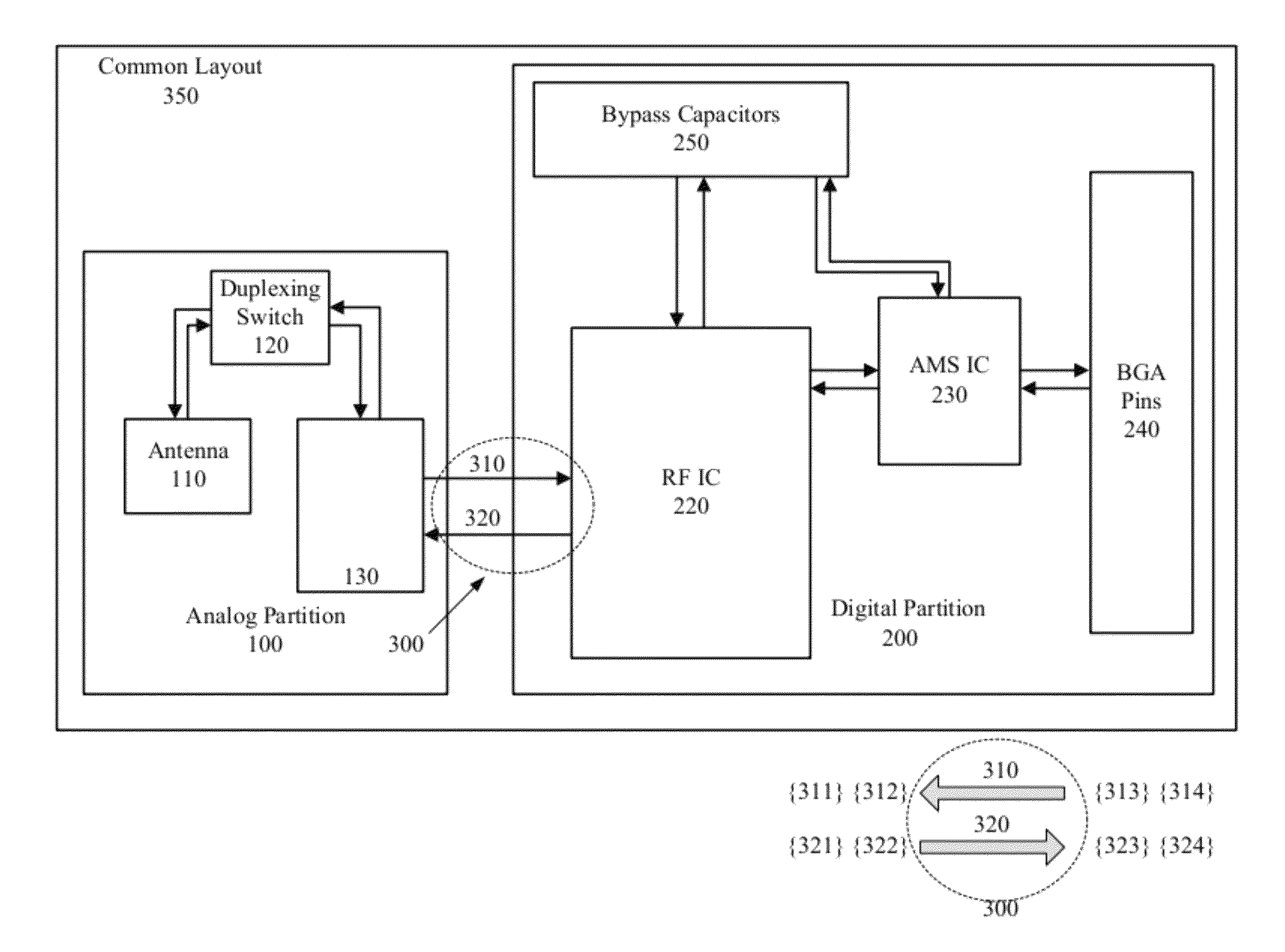
[0038]Reference will now be made in detail to the preferred embodiments of the invention, examples of which are illustrated in the accompanying drawings. The invention may, however, be embodied in many different forms and should not be construed as being limited to the embodiments set forth herein; rather, these embodiments are provided so that this disclosure will be thorough and complete, and will fully convey the concept of the invention to those skilled in the art. In the drawings, the thicknesses of layers and regions are exaggerated for clarity. Like reference numerals in the drawings denote like elements.

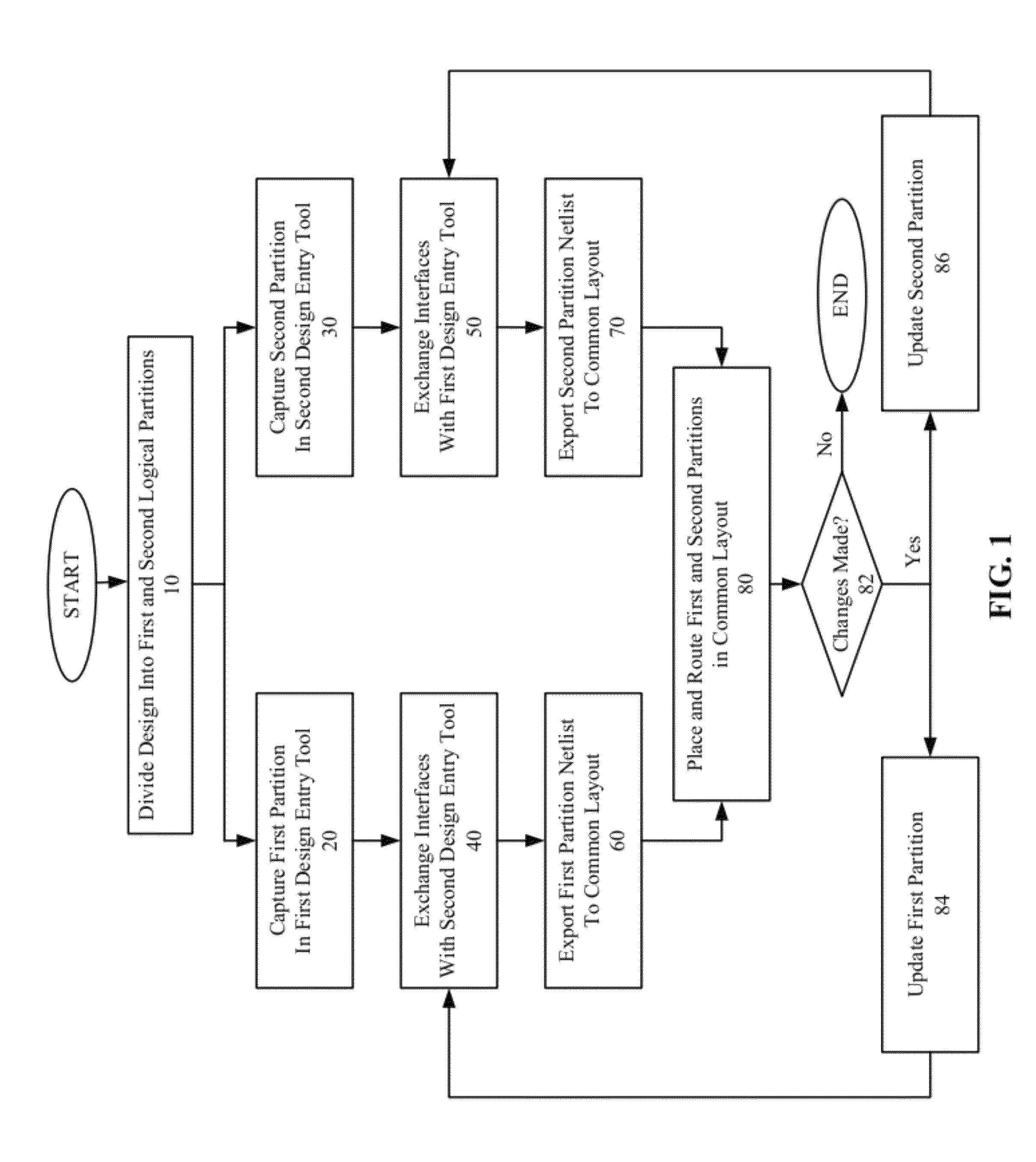
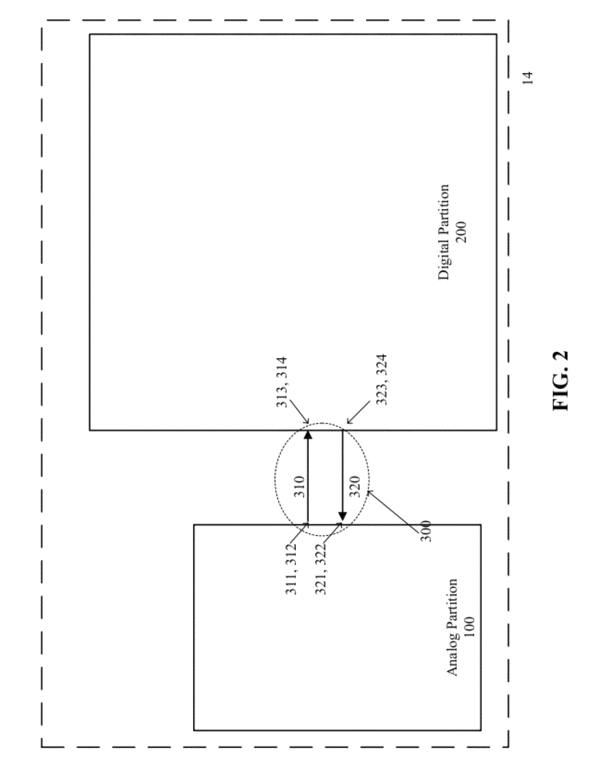
[0039]FIG. 1 shows an exemplary flowchart illustrating a method for concurrently designing an electronic circuit across different design entry tools according to an embodiment of the invention. Referring to FIG. 1, the design of an electronic circuit is divided into at least first and second logical partitions at an initial design stage 10. At this initial design stage 10, in...


PUM


Abstract

A method of interconnecting a first plurality of electronic components and a second plurality of electronic components to form an electronic circuit includes exporting a first netlist representing a first interconnection of the first electronic components in a first design entry tool, exporting a second netlist representing a second interconnection of the second electronic components in a second design entry tool, providing at least a first interface from the second plurality to the first plurality in the second design entry tool, populating the first interface through the first design entry tool, and exporting a third netlist representing the first interface from the second plurality to the first plurality from the second design entry tool, wherein the third netlist stitches the first netlist to the second netlist.

Description

BACKGROUND OF THE INVENTION[0001]1. Field of the Invention[0002]The embodiments of the invention relate to circuit design, and, more specifically, to design of an electronic circuit. Although embodiments of the invention are suitable for a wide scope of applications, it is particularly suitable for the concurrent design of electronic modules across different design entry tools targeted to a single layout.[0003]2. Discussion of the Related Art[0004]In general, an electronic circuit includes many electronic components and modules (e.g., antennae, transistors, diodes, inductors, capacitors, inverters, logic gates, multiplexers, integrated circuit (IC) chips, field programmable gate arrays (FPGAs) for performing various electronic functions). Each component or module is interconnected in a prescribed manner to respond to input electrical signals and produce other electrical signals according to the desired electronic function performed by the circuit. Some modules, such as ICs, system i...

Claims


Application Information

Patent Timeline
IPC IPC(8): G06F17/50G06F15/04
CPCG06F17/5045G06F2217/04G06F2111/02G06F30/30
Inventor KUKAL, TARANJITCHEUNG, CHRISKOHLI, VIKASFELTON, KEITHFARMAR, FRANK X.DURRILL, STEVEN R.
Owner CADENCE DESIGN SYST INC
Why Eureka
Try Eureka