Manufacturing method of semiconductor device including Au bump on seed film

a manufacturing method and semiconductor technology, applied in semiconductor devices, semiconductor/solid-state device details, electrical devices, etc., can solve the problems of shortening the plating time, reducing the hardness of the top part of the bump, and preventing height variation among the plurality of formed bumps, so as to achieve high current density and prevent height variation

Inactive Publication Date: 2012-11-27
RENESAS ELECTRONICS CORP
View PDF8 Cites 0 Cited by
  • Summary
  • Abstract
  • Description
  • Claims
  • Application Information

AI Technical Summary

Benefits of technology

[0009]In such a manufacturing method, a plurality of first Au bumps are formed by electrolytic plating with high current density, and the surfaces thereof are processed by grinding. A plurality of first Au bumps being formed by the electrolytic plating with high current density and having flat surfaces hardly arises a difference in dry etching of seed film so that it is possible to prevent height variation among the plurality of first Au bumps.

Problems solved by technology

Such a bump forming method can shorten the plating time and can also reduce the hardness of a top part of a bump.
A bump forming method by electrolytic plating may cause height variation among a plurality of formed bumps, due to nonuniformity of metal concentration caused by inadequate plating solution circulation or nonuniformity of electric field strength in the plating solution.
The height variation among the plurality of bumps is likely to cause connection failure upon bonding of the semiconductor chip and the wiring board, which leads to a risk of deteriorating reliability of the semiconductor device.

Method used


Image

  • Manufacturing method of semiconductor device including Au bump on seed film
  • Manufacturing method of semiconductor device including Au bump on seed film
  • Manufacturing method of semiconductor device including Au bump on seed film

Examples


first embodiment

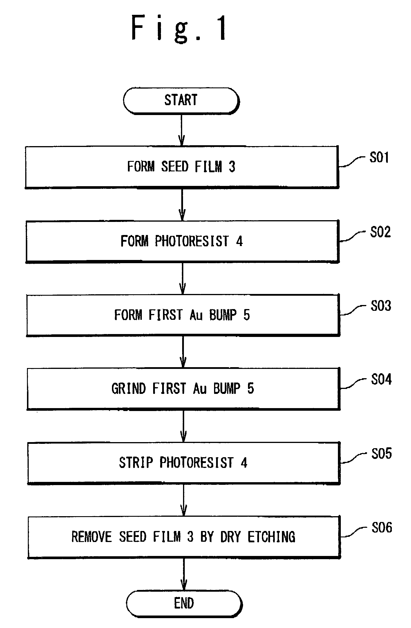
[0023]FIG. 1 is a flowchart showing the semiconductor device manufacturing method according to a first embodiment of the present invention. The first embodiment of the present invention will be described, referring to each of the processes shown in FIG. 1.

Step S01:

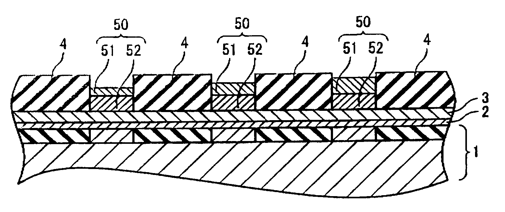
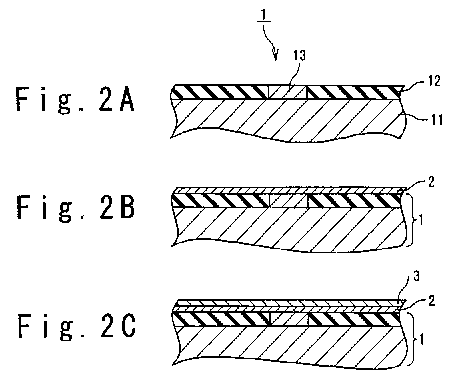
[0024]A seed film is formed on a semiconductor chip. FIGS. 2A, 2B, and 2C are diagrams showing some processes of forming a seed film 3 on a semiconductor chip 1. Referring to FIGS. 2A, 2B, and 2C, the process of forming the seed film 3 on the semiconductor chip 1 will be described. FIG. 2A is a partial sectional view of the semiconductor chip 1 where the seed film 3 is to be formed. Referring to FIG. 2A, the semiconductor chip 1 is provided with: a wafer 11, an insulation layer 12, and an electrode 13. On the silicon wafer 11, transistors and wirings are formed to realize various functions as the semiconductor chip 1. The insulation layer 12 covers the wafer 11 without covering the electrode 13 and prevents mutual contact ...

second embodiment

[0036]The semiconductor device manufacturing method according to a second embodiment of the present invention will be described. The second embodiment differs from the first embodiment in a method of forming an Au bump at an opening part 41. Therefore, components same as those of the first embodiment will be provided with the same numerals and overlapping description thereof will be omitted.

[0037]FIG. 9 is a flowchart showing the semiconductor device manufacturing method according to the second embodiment of the present invention. The second embodiment of the present invention will be described, referring to each of the processes shown in FIG. 9.

Step S10:

[0038]A seed film 3 is formed on a semiconductor chip 1 (see FIG. 2C, and similar to step S01 of the first embodiment).

Step S11:

[0039]A photoresist 4 having the opening part 41 above an electrode 13 of the semiconductor chip 1 is formed on the seed film 3 (see FIG. 3, and similar to step S02 of the first embodiment).

Step S12:

[0040]B...


PUM


Abstract

The manufacturing method includes: forming a seed film on a semiconductor chip; forming a photoresist having an opening above an electrode of the semiconductor chip on the seed film; forming a first Au bump on the seed film in the opening by electrolytic plating with a current density of 1.5 A / dm2 or above; grinding a surface of the first Au bump; stripping the photoresist; and removing the seed film by dry-etching.

Description

INCORPORATION BY REFERENCE[0001]This patent application is based on Japanese Patent Application No. 2009-155369. The disclosure of the Japanese Patent Application is incorporated herein by reference.BACKGROUND OF THE INVENTION[0002]1. Field of the Invention[0003]The present invention relates to a semiconductor device manufacturing method and more specifically to a bump forming method.[0004]2. Description of Related Art[0005]As a method of connecting a semiconductor chip and a wiring board in a semiconductor device manufacturing process, there is a method called gang bonding by which projecting electrodes (hereinafter referred to as bumps) of, for example, Au, solder, or Cu formed on the semiconductor chip and leads of the wiring board are collectively connected together. The gang bonding is also widely used in COG (Chip On Glass) in which a semiconductor chip is directly attached to a glass substrate. For the gang bonding, the following kinds of bump are used: a stud bump used in a ...

Claims


Application Information

Patent Timeline
Patent Type & Authority Patents(United States)
IPC IPC(8): H01L21/44
CPCH01L24/11H01L24/03H01L2924/01013H01L2924/0002H01L2924/15788H01L2224/0401H01L2224/1184H01L2224/05023H01L2224/05568H01L2924/014H01L2924/01006H01L2924/01005H01L2924/00013H01L2224/94H01L2224/13144H01L2224/13023H01L2224/11912H01L2224/11902H01L2224/1147H01L2224/11462H01L2224/05644H01L2224/05166H01L2224/0361H01L2224/0345H01L24/13H01L24/05H01L2924/01082H01L2924/01022H01L2924/01029H01L2924/01033H01L2924/01047H01L2924/01078H01L2924/01079H01L2224/11H01L2924/00014H01L2924/01074H01L2224/13099H01L2224/05099H01L2224/13599H01L2224/05599H01L2224/29099H01L2224/29599H01L2224/05552H01L2924/00
Inventor OKAJI, SHIGEHARU
Owner RENESAS ELECTRONICS CORP
Why Eureka
Try Eureka