Laterally diffused metal-oxide-semiconductor device

a metal-oxide-semiconductor and lateral diffusion technology, which is applied in the direction of semiconductor devices, basic electric elements, electrical appliances, etc., can solve the problems of increasing the transition time of the voltage, reducing the integration degree of the device, and increasing the voltage resistance, so as to reduce the electric field and improve the voltage resistance ability, the effect of laterally diffused metal-oxide-semiconductor devices

Active Publication Date: 2012-11-27
SINOPOWER SEMICON
View PDF7 Cites 4 Cited by
  • Summary
  • Abstract
  • Description
  • Claims
  • Application Information

AI Technical Summary

Benefits of technology

[0010]The laterally diffused metal-oxide-semiconductor device of the present invention utilize the source polysilicon layer, which is disposed on the gate dielectric layer above the drain region, to serve as a field plate for reducing the electric field. The voltage-withstand ability of the laterally diffused metal-oxide-semiconductor device can be improved, and the laterally diffused metal-oxide-semiconductor device can have a higher breakdown voltage. Also, the source polysilicon layer can effectively increase the drain-to-source capacitance and improve the output capacitance. Furthermore, the present invention can effectively decrease the gate-to-drain capacitance and reduce the input capacitance and the reverse transfer capacitance. In addition, by the first drain contact plug, the present invention can improve the drain-to-source on-resistance to reduce the power loss. Moreover, the present invention can effectively reduce the horizontal extension length and increase the integration degree of the device.

Problems solved by technology

However, increasing the horizontal extension length of the device not only decreases the integration degree of the device, but also increases the on-resistance of the device.
Accordingly, when the trench semiconductor device is applied to the switching device, this high gate-to-drain capacitance will increase the transition time of the voltage and influences the power loss.

Method used


Image

  • Laterally diffused metal-oxide-semiconductor device
  • Laterally diffused metal-oxide-semiconductor device
  • Laterally diffused metal-oxide-semiconductor device

Examples


Embodiment Construction

[0020]In the following specifications and claims, certain terms are used throughout the description and following claims to refer to particular components. As one skilled in the art will appreciate, electronic equipment manufacturers may refer to a component by different names. This document does not intend to distinguish between components that differ in name but not function. In the following description and in the claims, the terms “include” and “comprise” are used in an open-ended fashion, and thus should be interpreted to mean “include, but not limited to”. Also, the term “electrically connect” is intended to mean either an indirect or direct electrical connection. Accordingly, if one device is coupled to another device, that connection may be through a direct electrical connection, or through an indirect electrical connection via other devices and connections.

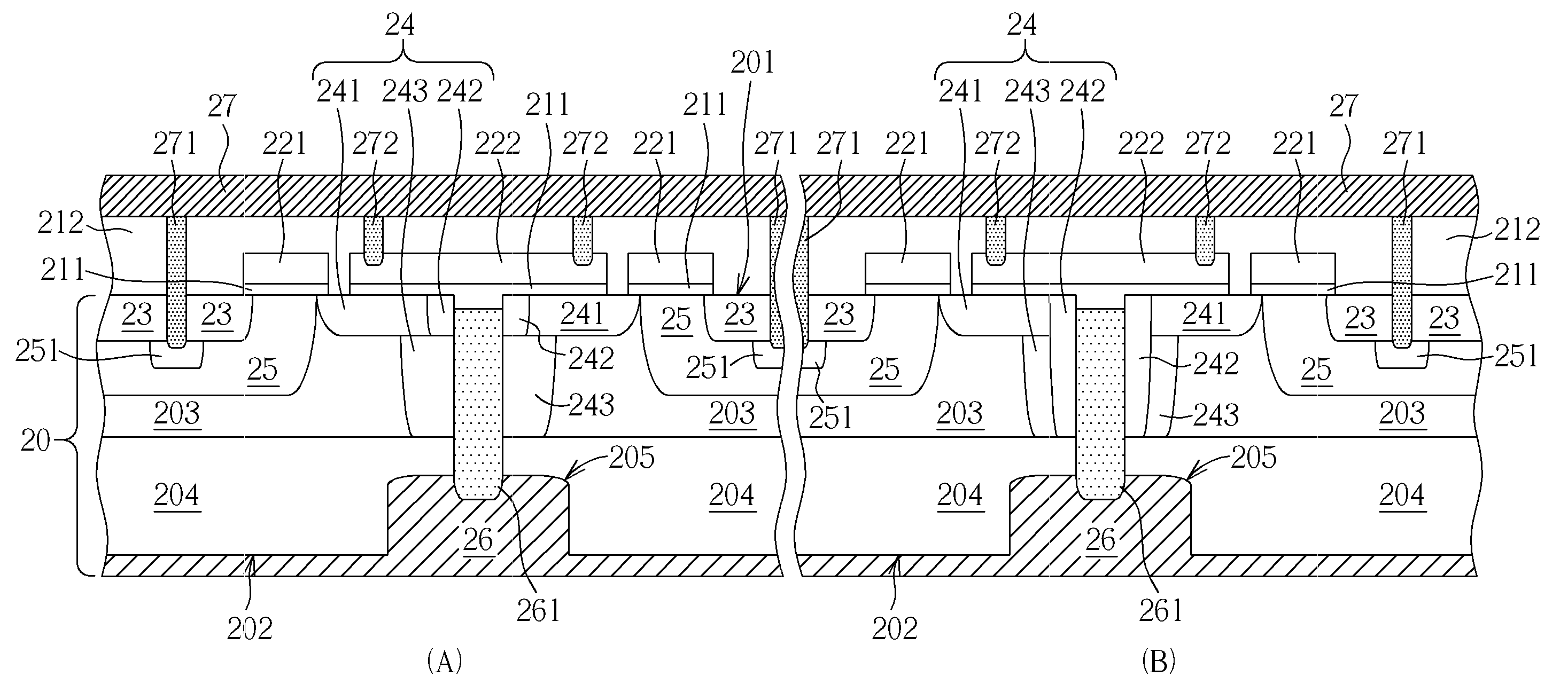
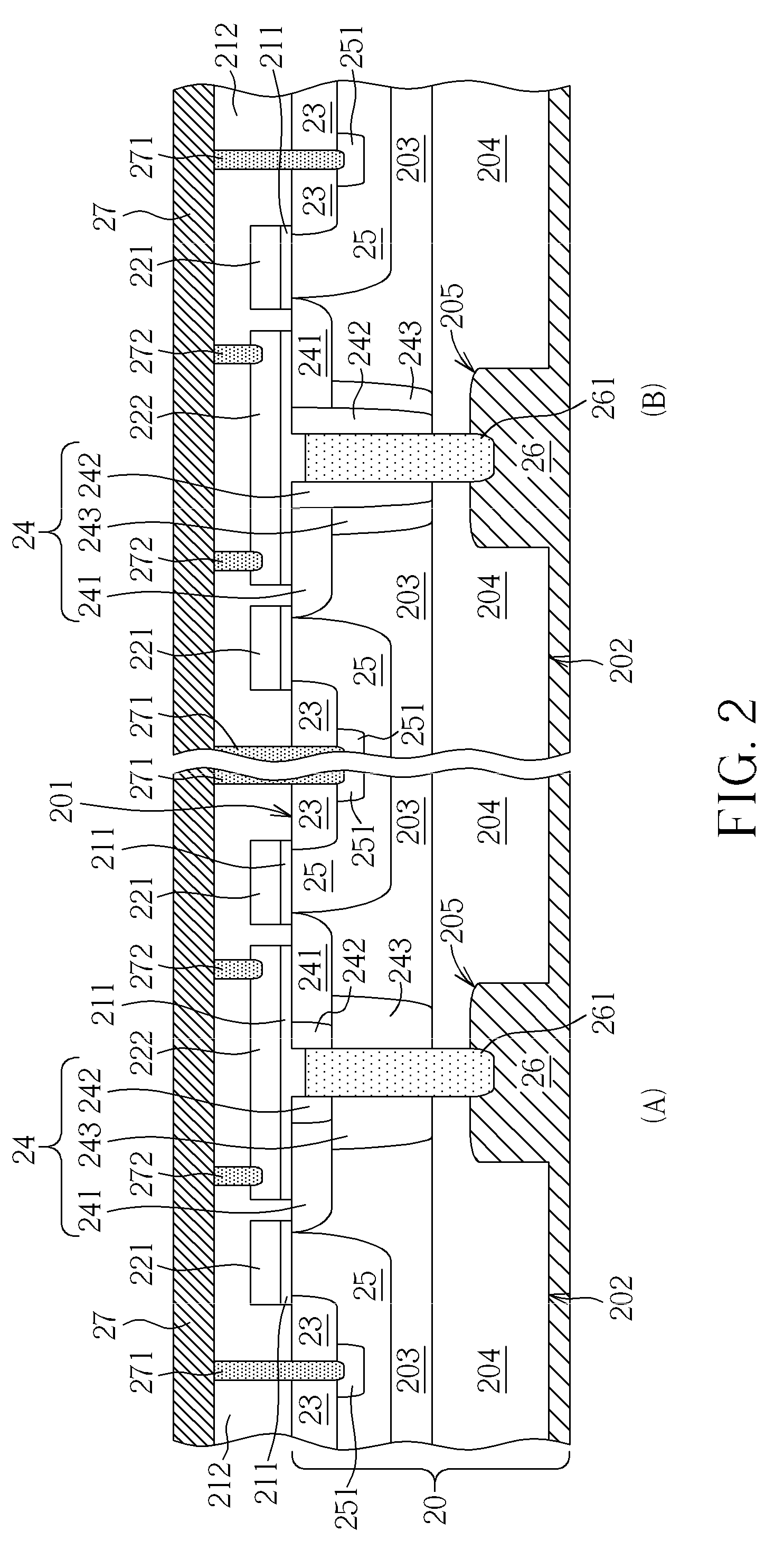
[0021]Please refer to FIG. 2, which is a schematic cross-sectional view illustrating a laterally diffused metal-oxide-s...


PUM


Abstract

A laterally diffused metal-oxide-semiconductor device includes a substrate, a gate dielectric layer, a gate polysilicon layer, a source region, a drain region, a body region, a first drain contact plug, a source polysilicon layer, an insulating layer, and a source metal layer. The source polysilicon layer disposed on the gate dielectric layer above the drain region can serve as a field plate to enhance the breakdown voltage and to increase the drain-to-source capacitance. In addition, the first drain contact plug of the present invention can reduce the drain-to-source on-resistance and the horizontal extension length.

Description

BACKGROUND OF THE INVENTION[0001]1. Field of the Invention[0002]The present invention relates to a laterally diffused metal-oxide-semiconductor device, and more particularly to a laterally diffused metal-oxide-semiconductor device which can improve capacitance characteristics with the optimized on-resistance.[0003]2. Description of the Prior Art[0004]A laterally diffused metal-oxide-semiconductor (LDMOS) device is a common semiconductor power device. Due to the horizontal structure of the laterally diffused metal-oxide-semiconductor device, it is easily formed and integrated with the conventional semiconductor techniques so as to reduce the manufacturing cost. Since the laterally diffused metal-oxide-semiconductor device has a higher breakdown voltage and a higher output power, it is widely applied to the electronic devices, such as a power converter, a power amplifier, a switch, and a rectifier.[0005]Please refer to FIG. 1, which is a schematic cross-sectional view illustrating a l...

Claims


Application Information

Patent Timeline
Patent Type & Authority Patents(United States)
IPC IPC(8): H01L29/66
CPCH01L29/41725H01L29/41766H01L29/7816H01L29/0878H01L29/402H01L29/7835H01L29/41758H01L29/4175H01L29/0847H01L29/0657H01L29/456
Inventor LIN, WEI-CHIEHCHEN, HO-TAILIN, JIA-FULI, PO-HSIEN
Owner SINOPOWER SEMICON
Why Eureka
Try Eureka