
Semiconductor device and driving method of the same

a technology of semiconductor devices and driving methods, applied in semiconductor devices, digital storage, instruments, etc., can solve the problems of increasing the cost per storage capacity, difficult to adequately reduce power consumption, short data holding period, etc., and achieve the effect of reducing power consumption

Active Publication Date: 2012-11-27
SEMICON ENERGY LAB CO LTD
View PDF146 Cites 8 Cited by
  • Summary
  • Abstract
  • Description
  • Claims
  • Application Information

AI Technical Summary

Benefits of technology

The semiconductor device achieves significant reductions in power consumption, eliminates the need for high voltage operations, and enhances reliability by maintaining data retention for extended periods without power, while allowing for high-speed data writing and erasure operations.

Problems solved by technology

Moreover, since leakage current (off-state current) flows between a source and a drain of a transistor included in a memory element when the transistor is in an off state, charge flows into or out even if the transistor is not selected, which makes a data holding period short.
For that reason, another writing operation (refresh operation) is necessary at predetermined intervals, and it is difficult to adequately reduce power consumption.
Furthermore, since stored data is lost when power supply stops, another memory device utilizing a magnetic material or an optical material is needed in order to hold the data for a long time.
However, cost per storage capacity is increased because a circuit such as a flip-flop is used.
Moreover, as in a DRAM, stored data in an SRAM is lost when power supply stops.
However, in a flash memory, there is a problem in that a memory element does not function after a predetermined number of writing operations because a gate insulating layer included in the memory element deteriorates due to tunneling current generated in writing operations.
Moreover, even when such a method is employed, the fundamental problem about the lifetime is not resolved.
In other words, a flash memory is not suitable for applications in which data is frequently rewritten.
Further, it takes a relatively long time to inject or remove charge, and it is not easy to increase a speed of writing and erasing data.

Method used


Image

  • Semiconductor device and driving method of the same
  • Semiconductor device and driving method of the same
  • Semiconductor device and driving method of the same

Examples


embodiment 1

(Embodiment 1)

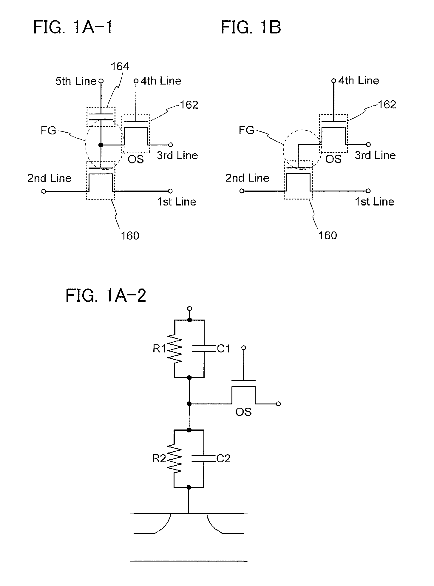
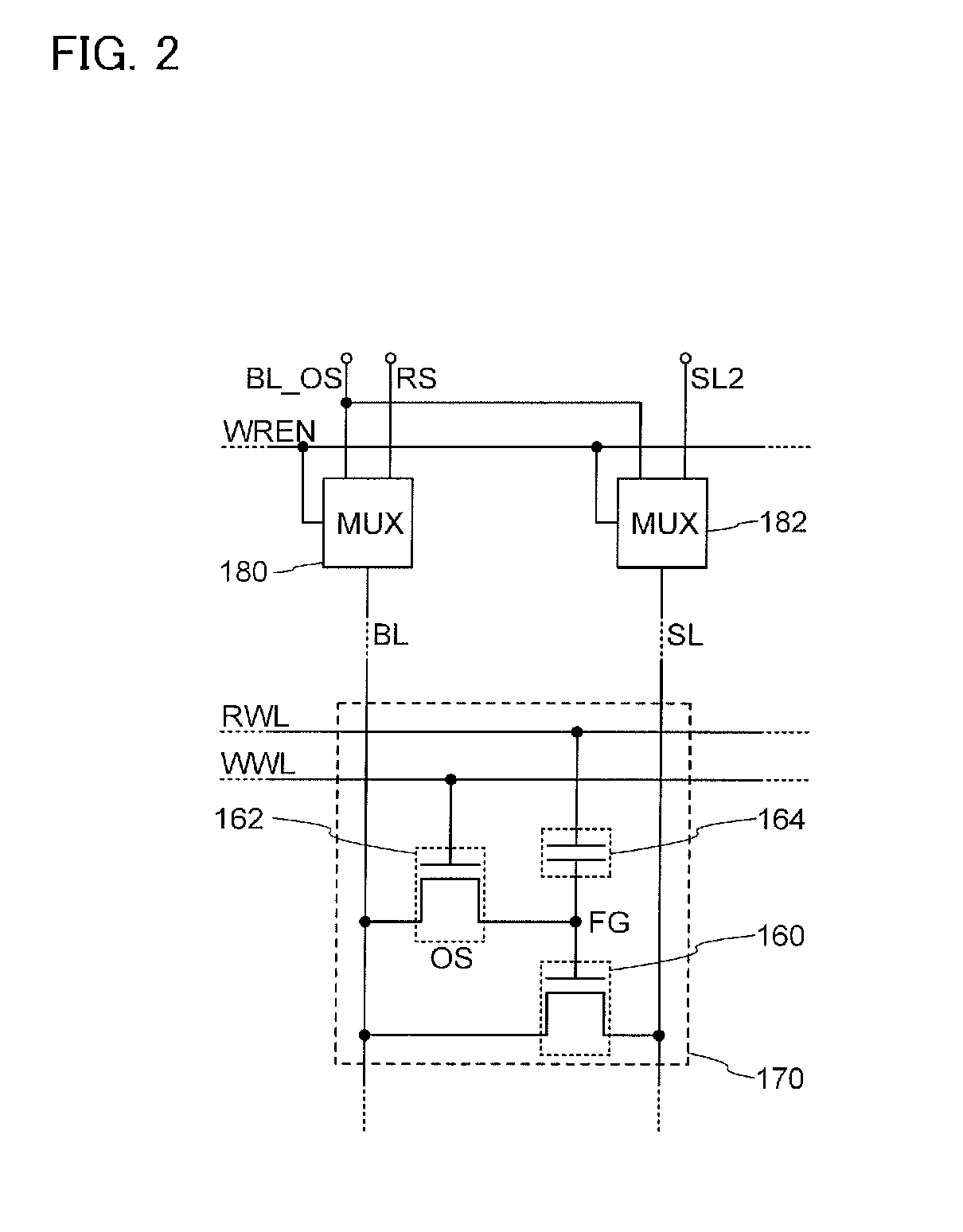
[0051]In this embodiment, a basic circuit structure and operation of a semiconductor device according to one embodiment of the disclosed invention will be described with reference to FIGS. 1A-1, 1A-2, and 1B and FIG. 2. Note that in each of the circuit diagrams, “OS” may be written beside a transistor in order to indicate that the transistor includes an oxide semiconductor.

[0052]First, the most basic circuit structure and its operation will be described with reference to FIGS. 1A-1, 1A-2, and 1B. In the semiconductor device in FIG. 1A-1, a first wiring. (a 1st line) and a source electrode (or a drain electrode) of a transistor 160 are electrically connected to each other, and a second wiring (a 2nd line) and the drain electrode (or the source electrode) of the transistor 160 are electrically connected to each other. In addition, a third wiring (a 3rd line) and a source electrode (or a drain electrode) of a transistor 162 are electrically connected to each other, and a ...

embodiment 2

(Embodiment 2)

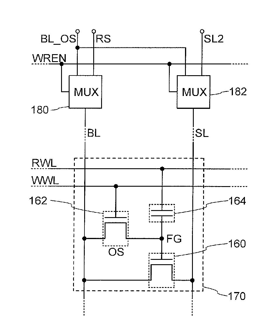
[0099]In this embodiment, an application example of the semiconductor device described in the above embodiment will be described. Specifically, an example of a semiconductor device in which the semiconductor devices described in the above embodiment are arranged in a matrix will be described with reference to FIGS. 3 and 4.

[0100]FIG. 3 illustrates an example of a circuit diagram of a semiconductor device including m×n memory cells 170.

[0101]The semiconductor device according to this embodiment includes m (m is an integral greater than or equal to 2) write word lines WWLs, m read word lines RWLs, n (n is an integral greater than or equal to 2) bit lines BLs, n source lines SLs, a memory cell array in which the memory cells 170 are arranged in a matrix of m rows (in a vertical direction)×n columns (in a horizontal direction), multiplexers 180 connected to respective n bit lines BLs, multiplexers 182 connected to respective n source lines SLs, a first driver circuit 190, ...

embodiment 3

(Embodiment 3)

[0114]In this embodiment, a structure and a manufacturing method of a semiconductor device according to an embodiment of the disclosed invention will be described with reference to FIGS. 5A and 5B, FIGS. 6A to 6D, FIGS. 7A to 7D, FIGS. 8 to 8D, and FIGS. 9A to 9C.

[0115]FIGS. 5A and 5B illustrate an example of a structure of a semiconductor device. FIG. 5A illustrates a cross section of the semiconductor device, and FIG. 5B illustrates a plan view of the semiconductor device. Here, FIG. 5A illustrates a cross section taken along line A1-A2 and line B1-B2 in FIG. 5B. The semiconductor device illustrated in FIGS. 5A and 5B includes the transistor 160 including a first semiconductor material in a lower portion, and the transistor 162 including a second semiconductor material in an upper portion. Here, the first semiconductor material and the second semiconductor material are preferably different from each other. For example, the first semiconductor material may be a semico...


PUM


Abstract

An object is to provide a semiconductor device with a novel structure in which stored data can be held even when power is not supplied, and the number of times of writing is not limited. The semiconductor device is formed using a wide gap semiconductor and includes a potential change circuit which selectively applies a potential either equal to or different from a potential of a bit line to a source line. Thus, power consumption of the semiconductor device can be sufficiently reduced.

Description

TECHNICAL FIELD[0001]The disclosed invention relates to a semiconductor device using a semiconductor element and a driving method thereof.BACKGROUND ART[0002]Memory devices using semiconductor elements are broadly classified into two categories: a volatile device that loses stored data when not powered, and a non-volatile device that holds stored data even when not powered.[0003]A typical example of a volatile memory device is a dynamic random access memory (DRAM). A DRAM stores data in such a manner that a transistor included in a memory element is selected and charge is accumulated in a capacitor.[0004]Owing to the above principle, charge in the capacitor is lost when data in a DRAM is read out; thus, another writing operation is necessary every time data is read out. Moreover, since leakage current (off-state current) flows between a source and a drain of a transistor included in a memory element when the transistor is in an off state, charge flows into or out even if the transis...

Claims


Application Information

Patent Timeline
Patent Type & Authority Patents(United States)
IPC IPC(8): G11C11/24H10B12/00H10B69/00
CPCG11C11/403H01L27/1052H01L27/1225G11C11/24G11C11/405H01L27/11521H10B41/30H10B41/70
Inventor INOUE, HIROKIKATO, KIYOSHIMATSUZAKI, TAKANORINAGATSUKA, SHUHEI
Owner SEMICON ENERGY LAB CO LTD
Learn More