Driving method of semiconductor device

a driving method and semiconductor technology, applied in static storage, digital storage, instruments, etc., can solve the problems of short data holding period, difficult to sufficiently reduce power consumption, and loss of stored data, so as to achieve the effect of reducing power consumption, storing data for an extremely long time, and avoiding data loss

Active Publication Date: 2012-12-25
SEMICON ENERGY LAB CO LTD
View PDF19 Cites 4 Cited by
  • Summary
  • Abstract
  • Description
  • Claims
  • Application Information

AI Technical Summary

Benefits of technology

[0013]In the disclosed invention, a semiconductor device is formed using a material which allows a sufficient reduction in off-state current of a transistor; for example, an oxide semiconductor material, which is a wide-gap semiconductor, is used. When a semiconductor material which allows a sufficient reduction in off-state current of a transistor is used, the semiconductor device can hold data for a long period.
[0027]Since the off-state current of a transistor including an oxide semiconductor is extremely small, stored data can be held for an extremely long time by using the transistor. In other words, power consumption can be adequately reduced because a refresh operation becomes unnecessary or the frequency of refresh operations can be extremely low. Moreover, stored data can be held for a long period even when power is not supplied (note that a potential is preferably fixed).
[0028]Further, a semiconductor device according to an embodiment of the disclosed invention does not need high voltage for writing of data and there is no problem of deterioration of elements. For example, unlike a conventional non-volatile memory, it is not necessary to inject and extract electrons into and from a floating gate, and thus a problem such as deterioration of a gate insulating layer does not occur at all. In other words, the semiconductor device according to an embodiment of the disclosed invention does not have a limitation on the number of times of writing operations which is a problem in a conventional non-volatile memory, and reliability is drastically improved. Furthermore, data is written depending on the on state and the off state of the transistor, whereby a high-speed operation can be easily realized. In addition, there is no need of an operation for erasing data.
[0029]When a transistor which includes a material other than an oxide semiconductor and can operate at sufficiently high speed is used as a reading transistor in combination with a transistor which includes an oxide semiconductor and is used as a writing transistor, a semiconductor device can perform an operation (e.g., a data reading operation) at sufficiently high speed. Further, with a transistor including a material other than an oxide semiconductor, a variety of circuits (such as a logic circuit and a driver circuit) which are required to operate at high speed can be favorably realized.

Problems solved by technology

Moreover, for example, since leakage current (off-state current) flows between a source and a drain of a transistor included in a storage element when the transistor is in an off state, electric charge flows into or out even if the transistor is not selected, which makes a data holding period short.
For that reason, another writing operation (refresh operation) is necessary at predetermined intervals, and it is difficult to sufficiently reduce power consumption.
Furthermore, since stored data is lost when power is not supplied, an additional storage device using a magnetic material or an optical material is needed in order to hold data for a long time.
However, cost per storage capacity is increased because a circuit such as a flip-flop is used.
Moreover, as in a DRAM, stored data in an SRAM is lost when power is not supplied.
However, a gate insulating layer included in a storage element deteriorates by tunneling current generated in writing, so that the storage element stops its function after a predetermined number of writing operations.
However, a complicated peripheral circuit is needed to realize this method.
Moreover, employing such a method does not solve the fundamental problem of lifetime.
In other words, a flash memory is not suitable for applications in which data is frequently rewritten.
Further, it takes a relatively long time to inject or remove electric charge, and it is not easy to increase the speed of writing and erasing of data.

Method used


Image

  • Driving method of semiconductor device
  • Driving method of semiconductor device
  • Driving method of semiconductor device

Examples


embodiment 1

[0051]In this embodiment, a basic circuit structure and an operation of a semiconductor device according to an embodiment of the disclosed invention will be described with reference to FIGS. 1A and 1B and FIGS. 2A and 2B. Note that in each of circuit diagrams, in some cases, “OS” is written beside a transistor in order to indicate that the transistor includes an oxide semiconductor.

1>

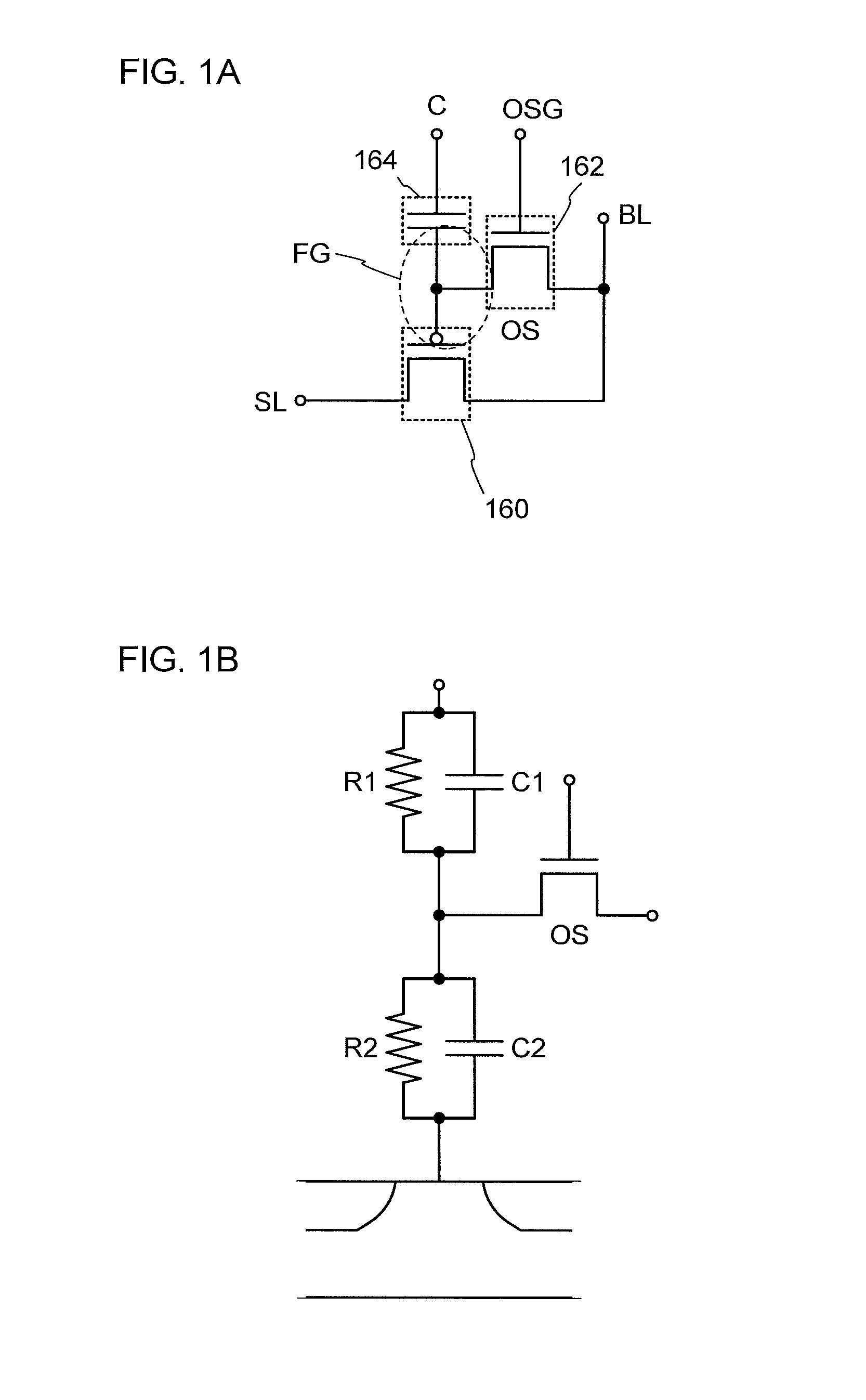
[0052]First, the most basic circuit structure and its operation are described with reference to FIGS. 1A and 1B. In a semiconductor device illustrated in FIG. 1A, a bit line BL, a source electrode (or a drain electrode) of a transistor 160, and a source electrode (or a drain electrode) of a transistor 162 are electrically connected to each other; and a source line SL and the drain electrode (or the source electrode) of the transistor 160 are electrically connected to each other. In addition, a write word line OSG and a gate electrode of the transistor 162 are electrically connected to each other. A gate...

application example 1

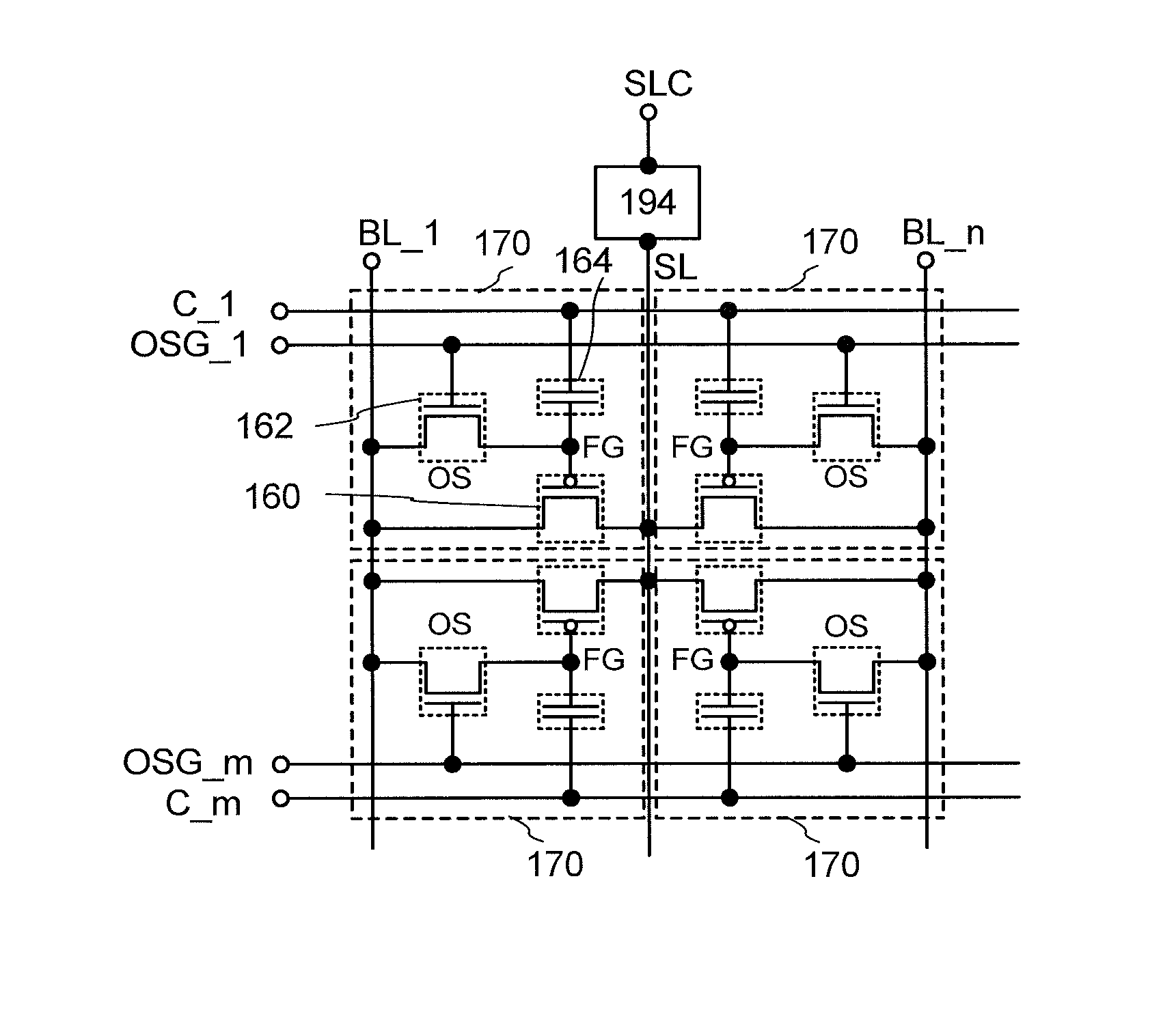
[0113]Next, a more specific circuit structure to which the circuit illustrated in FIGS. 1A and 1B is applied will be described with reference to FIG. 4 and FIGS. 5A to 5D. Note that the case where an n-channel transistor is used as the writing transistor (the transistor 162) and a p-channel transistor is used as the reading transistor (the transistor 160) will be described below as an example. Note that in the circuit diagram illustrated in FIG. 4, wirings with slashes are wirings each including a plurality of signal lines.

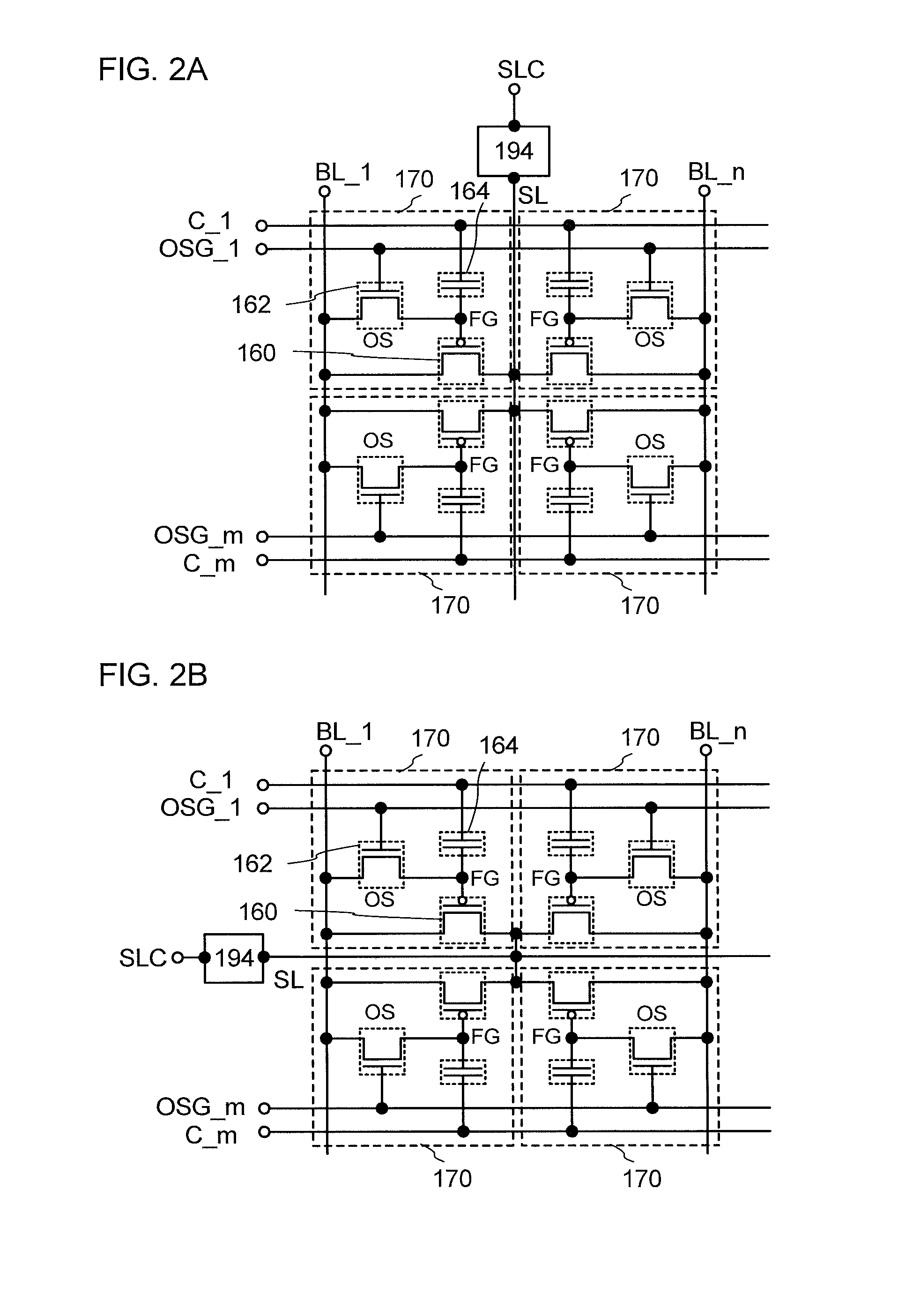
[0114]FIG. 4 is an example of a circuit diagram of a semiconductor device including (m×n) memory cells 170. The structure of the memory cells 170 in FIG. 4 is similar to that in FIG. 1A.

[0115]The semiconductor device illustrated in FIG. 4 includes m (m is an integer of greater than or equal to 2) write word lines OSG; m write-read word lines C, n (n is an integer of greater than or equal to 2) bit lines BL, a source line SL, a memory cell array having the memory c...

embodiment 2

[0129]In this embodiment, a structure and a manufacturing method of a semiconductor device according to an embodiment of the disclosed invention will be described with reference to FIGS. 6A and 6B, FIGS. 7A to 7G, FIGS. 8A to 8E, FIGS. 9A to 9D, FIGS. 10A to 10D, and FIGS. 11A to 11C.

[0130]FIGS. 6A and 6B illustrate one example of a structure of the semiconductor device. FIG. 6A is a cross-sectional view of the semiconductor device, and FIG. 6B is a plan view of the semiconductor device. Here, FIG. 6A corresponds to a cross-section taken along line A1-A2 and line B1-B2 of FIG. 6B. The semiconductor device illustrated in FIGS. 6A and 6B includes a transistor 160 including a first semiconductor material in a lower portion, and a transistor 162 including a second semiconductor material in an upper portion. Here, the first semiconductor material is preferably different from the second semiconductor material. For example, a semiconductor material other than an oxide semiconductor can be ...


PUM


Abstract

A semiconductor device with a novel structure and a driving method thereof are provided. A semiconductor device includes a non-volatile memory cell including a writing transistor including an oxide semiconductor, a reading p-channel transistor including a semiconductor material different from that of the writing transistor, and a capacitor. Data is written to the memory cell by turning on the writing transistor so that a potential is supplied to a node where a source electrode of the writing transistor, one electrode of the capacitor, and a gate electrode of the reading transistor are electrically connected, and then turning off the writing transistor so that a predetermined amount of electric charge is held in the node. In a holding period, the memory cell is brought into a selected state and a source electrode and a drain electrode of the reading transistor are set to the same potential, whereby the electric charge stored in the node is held.

Description

BACKGROUND OF THE INVENTION[0001]1. Field of the Invention[0002]An embodiment of the disclosed invention relates to a semiconductor device including a semiconductor element and a driving method of the semiconductor device.[0003]2. Description of the Related Art[0004]Storage devices including semiconductor elements are broadly classified into two categories: a volatile device that loses stored data when power is not supplied, and a non-volatile device that holds stored data even when power is not supplied.[0005]A typical example of a volatile storage device is a DRAM (dynamic random access memory). A DRAM stores data in such a manner that a transistor included in a storage element is selected and electric charge is stored in a capacitor.[0006]When data is read from a DRAM, electric charge in a capacitor is lost on the above-described principle; thus, another writing operation is necessary whenever data is read out. Moreover, for example, since leakage current (off-state current) flow...

Claims


Application Information

Patent Timeline
Patent Type & Authority Patents(United States)
IPC IPC(8): G11C11/24
CPCG11C11/404G11C16/0433H01L27/1214
Inventor INOUE, HIROKIKATO, KIYOSHIMATSUZAKI, TAKANORINAGATSUKA, SHUHEI
Owner SEMICON ENERGY LAB CO LTD
Why Eureka
Try Eureka