Supercharge Your Innovation With Domain-Expert AI Agents!

Package system with a shielded inverted internal stacking module and method of manufacture thereof

a technology of shielded inverter and stacking module, which is applied in the direction of electrical apparatus, semiconductor device details, semiconductor/solid-state device devices, etc., can solve the problems of increasing the risk of damage during manufacturing, ic density remains limited, and the bulky multi-chip modul

Active Publication Date: 2012-12-18
STATS CHIPPAC LTD
View PDF15 Cites 7 Cited by
  • Summary
  • Abstract
  • Description
  • Claims
  • Application Information

AI Technical Summary

Benefits of technology

The present invention provides a method and system for manufacturing a package system that includes a base package substrate, an internal stacking module, and an electromagnetic interference shield. The method involves covering the internal stacking module with the electromagnetic interference shield, mounting the internal stacking module over the base package substrate, and then encapsulating at least portions of the internal stacking module, the electromagnetic interference shield, and the base package substrate using a second encapsulant. The technical effect of this invention is to provide a package system that can effectively shield against electromagnetic interference, which can improve the performance and reliability of the package system.

Problems solved by technology

The increasing functionality and decreasing size and number of system components make IC's increasingly susceptible to damage during manufacturing and in use.
However, IC density continues to be limited by the space (or “real estate”) available for mounting individual die on a base leadframe.
However, such multi-chip modules can be bulky.
Combining them into a single horizontal layer used board space inefficiently by consuming large base package substrate areas, and afforded less advantage in circuit miniaturization.
However, multi-chip modules, whether vertically or horizontally arranged, can also present problems because they usually must be assembled before the component chips and chip connections can be tested.
That is, because the electrical bond pads on a die are so small, it is difficult to test die before assembly onto a base package substrate.
With conventional multi-chip modules, however, the die cannot be individually identified as KGD before final assembly, leading to KGD inefficiencies and assembly process problems including yield.
Even though a shielded module may provide overall EMI protection from outside interference, semiconductor devices inside the module can still interfere with each other.
The main issues with existing shielding approaches are the lack of lateral shielding of the semiconductor die and lack of an effective and reliable approach for connecting the shield to a ground loop using the least number of lead connections.
Solutions to these problems have been long sought but prior developments have not taught or suggested any solutions and, thus, solutions to these problems have long eluded those skilled in the art.

Method used


Image

  • Package system with a shielded inverted internal stacking module and method of manufacture thereof
  • Package system with a shielded inverted internal stacking module and method of manufacture thereof
  • Package system with a shielded inverted internal stacking module and method of manufacture thereof

Examples


first embodiment

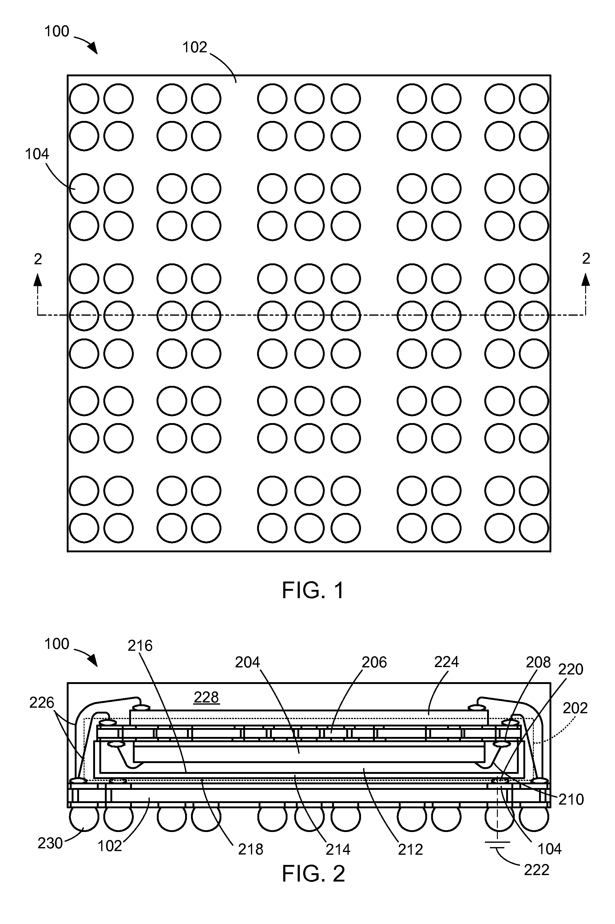
[0038]Referring now to FIG. 1, therein is shown a bottom plan view of a package system 100 in the present invention. In the bottom plan view only a base package substrate 102 is visible. The base package substrate is made of an insulating material and contains conductive elements 104 such as contact pads, connecting lines, and through vias.

[0039]Referring now to FIG. 2, therein is shown a cross-sectional view of the package system 100 taken along line 2-2 in FIG. 1. The package system 100 includes an internal stacking module 202 having a semiconductor die 204 attached to a package substrate 206. The semiconductor die 204 is electrically connected to conductive elements 208 in the package substrate 206 using interconnects 210 such as wire bonds. At least portions of the semiconductor die 204, the package substrate 206, and the interconnects are encapsulated using a first encapsulant 212.

[0040]The exposed regions of the first encapsulant 212 in the internal stacking module 202 are cov...

second embodiment

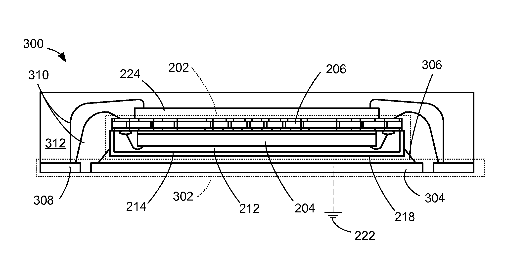
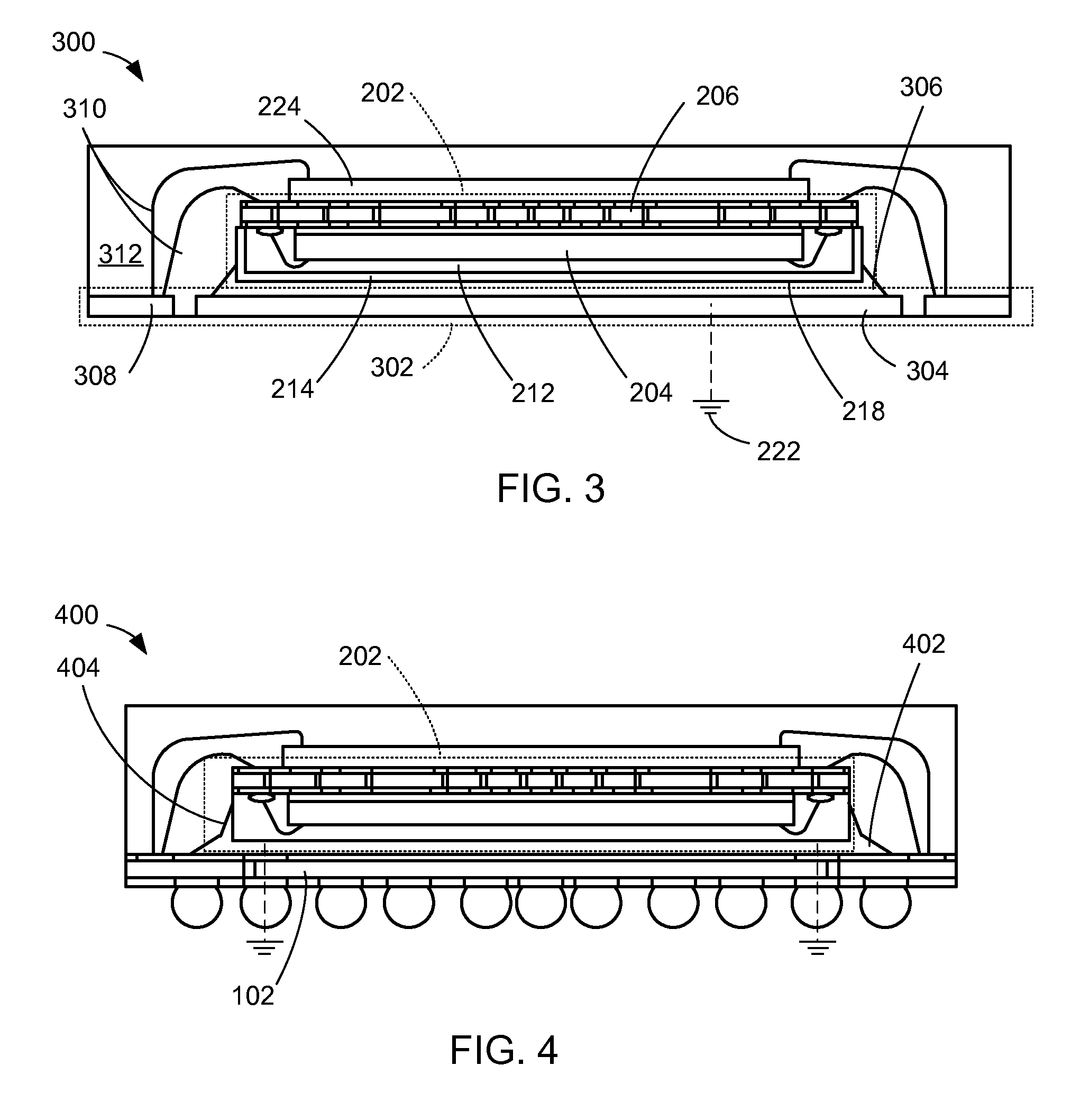
[0049]Referring now to FIG. 3, therein is shown a cross-sectional view of a package system 300 in the present invention. Similar to the package system 100 of FIG. 1, the package system 300 incorporates the internal stacking module 202 with an electromagnetic interference shield 214 covering exposed regions of the first encapsulant 212. The electromagnetic interference shield 214, isolates the semiconductor die 204 from electromagnetic interference generated within or outside the package system 300.

[0050]The internal stacking module 202 is mounted inverted over a leadframe 302, which replaces the base package substrate 102 in the package system 100 shown in FIG. 1. The outside face 218 of the electromagnetic interference shield 214 is attached to a die paddle 304 in the leadframe 302 using a conductive layer 306 such as solder or conductive epoxy paste. The die paddle 304, which is made of a conductive material, is in turn connected to the ground 222 outside the package system 300.

[0...

third embodiment

[0052]Referring now to FIG. 4, therein is shown a cross-sectional view of a package system 400 in the present invention. The package system 400 incorporates the internal stacking module 202 attached to the base package substrate 102 using a conductive layer 402 with a fillet 404 configured to be cover the sides of the internal stacking module 202 high enough as to act as an electromagnetic interference shield.

[0053]It has been discovered that the conductive layer 402 with the fillet 404 provides appropriate electromagnetic interference shielding, making the conductive layer 402 an adequate replacement for the electromagnetic interference shield 214 of FIG. 1.


PUM


Abstract

A method of manufacture of a package system includes: providing a base package substrate having conductive elements; providing an internal stacking module having a semiconductor die mounted on a package substrate and a first encapsulant surrounding at least portions of the semiconductor die and the package substrate; covering at least portions of the first encapsulant in the internal stacking module with an electromagnetic interference shield, the electromagnetic interference shield shaped to have an outside face; mounting the internal stacking module over the base package substrate with the outside face of the electromagnetic interference shield facing the base package substrate; and encapsulating at least portions of the internal stacking module, the electromagnetic interference shield, and the base package substrate using a second encapsulant.

Description

TECHNICAL FIELD[0001]The present invention relates generally to an integrated circuit packaging system, and more particularly to a packaging system incorporating an internal stacking module.BACKGROUND ART[0002]Consumers continue to demand higher performance and lower cost electronic products incorporating an increasing number of features. These market demands have resulted in increased miniaturization of components and greater packaging density of integrated circuits (“IC's”). The increasing functionality and decreasing size and number of system components make IC's increasingly susceptible to damage during manufacturing and in use. Integrated circuit packages are commonly used to encase the IC and provides protection and electrical connectivity to external circuitry and components.[0003]IC devices—also known as semiconductor dies—are constructed from a silicon or gallium arsenide wafer through a process that comprises a number of deposition, masking, diffusion, etching, and implant...

Claims


Application Information

Patent Timeline
Patent Type & Authority Patents(United States)
IPC IPC(8): H01L21/00
CPCH01L23/3128H01L23/49816H01L23/49833H01L23/552H01L24/73H01L25/03H01L25/50H01L24/16H01L24/29H01L24/48H01L2224/13025H01L2224/48227H01L2224/48247H01L2224/73207H01L2224/73265H01L2225/0651H01L2924/01013H01L2924/01079H01L2924/01082H01L2924/14H01L2924/15311H01L2924/19107H01L2924/3025H01L2224/32225H01L2224/32245H01L2224/48465H01L2924/014H01L2224/45124H01L2224/16225H01L2224/14181H01L2924/00H01L2924/00012H01L2224/45144H01L2924/00014H01L24/45H01L2924/181H01L2924/00015H01L2224/05599
Inventor PAGAILA, REZA ARGENTYCAMACHO, ZIGMUND RAMIREZBATHAN, HENRY DESCALZO
Owner STATS CHIPPAC LTD
Features
  • R&D
  • Intellectual Property
  • Life Sciences
  • Materials
  • Tech Scout
  • Unparalleled Data Quality
  • Higher Quality Content
  • 60% Fewer Hallucinations
Learn More