
Method for testing semiconductor film, semiconductor device and manufacturing method thereof

a technology of crystallized semiconductors and manufacturing methods, applied in solid-state devices, nuclear engineering, nuclear elements, etc., can solve the problems of large variation in tft characteristics, large grain size, and large grain size, and achieve the effect of less time, sufficient reliability, and accurate results

Active Publication Date: 2013-01-01
SEMICON ENERGY LAB CO LTD
View PDF33 Cites 9 Cited by
  • Summary
  • Abstract
  • Description
  • Claims
  • Application Information

AI Technical Summary

Benefits of technology

The invention provides a method to quickly and reliably test a semiconductor film before it is sold. The method is cost-effective and can be applied to mass production. The technical effects of the patent include the development of a reliable and efficient method for testing semiconductor films, which reduces the time and expense required for production. The invention also includes a manufacturing method for making semiconductor films and a laser crystallization system that can reliably and efficiently bring products to market.

Problems solved by technology

Each of the suggested methods, however, also has a disadvantage in that only a threshold at which micro-crystallization occurs is obtained, an oxide film is required, and a distinct difference does not generate due to the crystallization.
In crystallizing a silicon film, a grain size becomes larger as more energy is applied; however, it becomes small rapidly when more than a certain energy is applied.
The variation in TFT characteristics is a substantial problem since it is a major factor having an influence on the reliability and performance of the final products.

Method used


Image

  • Method for testing semiconductor film, semiconductor device and manufacturing method thereof
  • Method for testing semiconductor film, semiconductor device and manufacturing method thereof
  • Method for testing semiconductor film, semiconductor device and manufacturing method thereof

Examples


embodiment mode 1

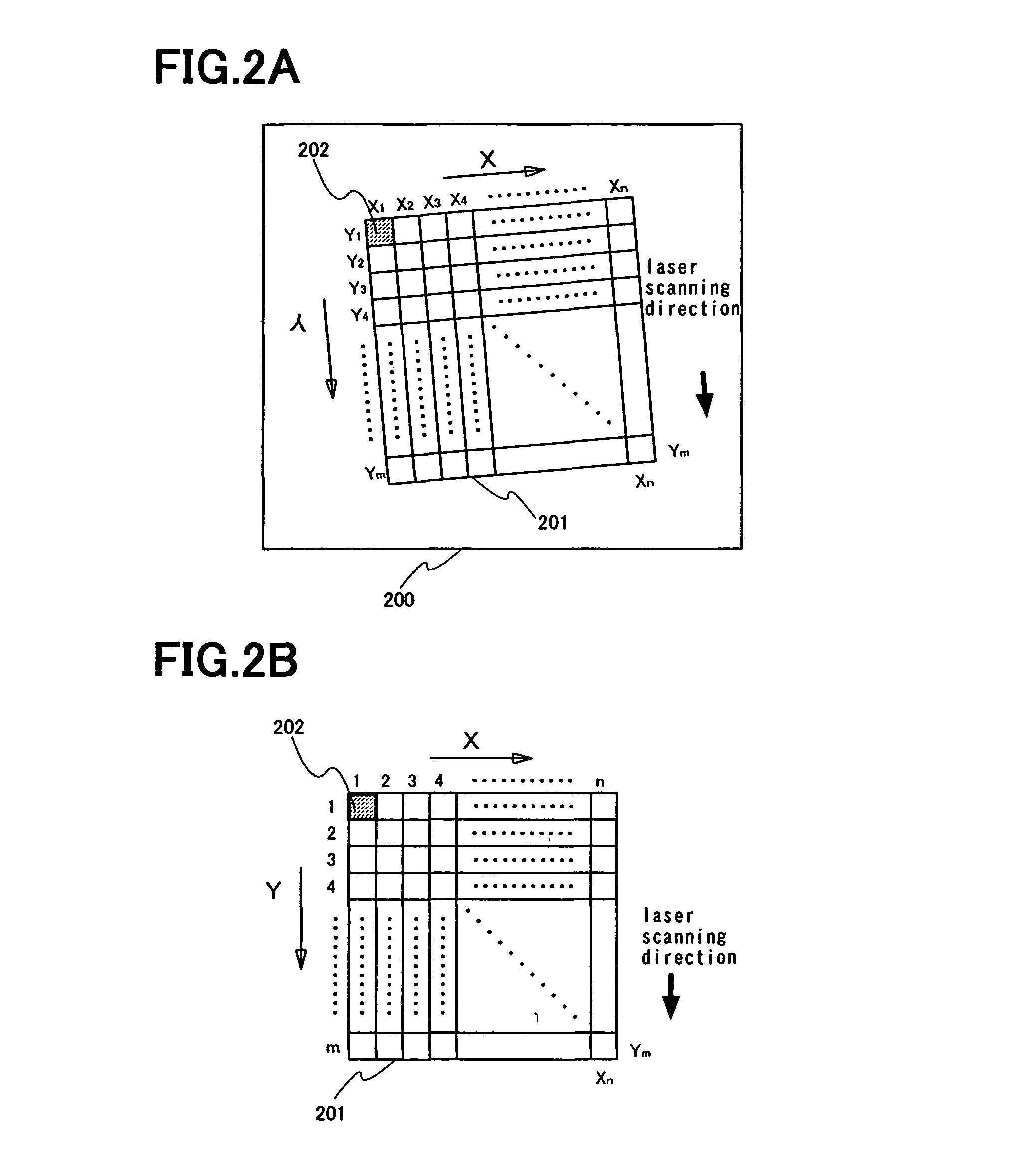
[0087][Image processing] An image processing commonly performed in the invention is described with reference to FIGS. 2A and 2B. In an image 200 photographed by a CCD camera and the like, it is defined that a scanning direction in which a laser beam is irradiated as energy beam for crystallization is a Y direction, and a direction perpendicular to the Y direction is an X direction.

[0088]An analysis region 201 is determined by sectioning the image in a predetermined size of rectangular shape of which two sides are parallel to the X direction and the other two sides are parallel to the Y direction. Here, in the case where the X direction or the Y direction is not parallel to the side of the image, the image analysis region 201 may be rotated by using an image processing software or the like. Further, the camera may be placed so that the image and the analysis region be parallel to each other.

[0089]The analysis region is divided into n in the X direction and into m in the Y direction, ...

embodiment mode 2

[0116]In this embodiment mode, a method for determining the irradiation energy density of an energy beam irradiation device by using the method for testing of the invention is described with reference to FIG. 6.

[0117]A substrate on which an amorphous semiconductor film is formed is irradiated for crystallization with an energy beam by changing the irradiation energy density (600) (irradiation energy density: E=1 to t). The energy density of the energy beam may be changed for each substrate or each sectioned area of the substrate.

[0118]Subsequently, each of the semiconductor films crystallized by each irradiation energy density is photographed by a CCD camera (601), and tested by the method described in the Methods for testing 1 to 3 (602). Values calculated after the analysis are compared to each other in their energy density (603) and the optimal crystallization energy density as seems best is determined (604). The optimal crystallization energy density as seems best is a condition...

embodiment mode 3

[0123]FIGS. 7 to 15 show the results of the measurement and testing of a substrate crystallized by actually using a laser beam. FIGS. 7 to 9 are dark field images photographed by a CCD camera. FIGS. 7A to 7K show 100 times magnification, FIGS. 8A to 8K show 200 times magnification, and FIGS. 9A to 9K show 500 times magnification image, each of which are reduced views in 16%. The actual testing was performed by analyzing the images of 100, 200, and 500 times magnification before the reduction in 16%. The laser irradiation energy density of each of the images No. 1 to 11 is shown in the following table 1.

[0124][Table 1]

[0125]

TABLE 1Image No.energy density [mJ / cm2]1  379 (−12.40%)2390.3 (−9.80%)3404.5 (−6.52%)4411.2 (−4.97%)5423.9 (−2.03%)7443.6 (+2.519%)8455.7 (+5.32%)9466.3 (+7.77%)10475.4 (+9.87%)11487.2 (+12.60%)underline; image regarded as optimal

[0126]When these images are tested by a sensory test, an image of which irradiated energy density seems optimal is No. 6 in the case of ...


PUM

PropertyMeasurementUnit
thicknessaaaaaaaaaa
thicknessaaaaaaaaaa
thicknessaaaaaaaaaa

Abstract

The invention provides a method for testing a semiconductor film, a manufacturing method of a semiconductor film, a laser crystallization method, a laser crystallization device, and a laser crystallization system, for testing a laser crystallized semiconductor film, which require less time, have sufficient reliability, are excellent in cost management and applicable to mass production. In the method for testing a semiconductor film having an improved crystallinity by irradiating an energy light, the tested semiconductor film is photographed in a dark field digital image and then the luminance of the digital image is calculated by a computer in a constant direction for testing.

Description

BACKGROUND OF THE INVENTION[0001]1. Field of the Invention[0002]The invention relates to a method for testing a crystallized semiconductor film, and more particularly such a method for testing a semiconductor film crystallized by irradiating an energy beam. The invention also relates to a device for testing a semiconductor film crystallized by irradiating an energy beam, and a manufacturing method of a semiconductor device including a step of testing a semiconductor film crystallized by irradiating an energy beam.[0003]2. Description of the Related Art[0004]A glass substrate is cheap and easily used in a large size as compared to a conventional single crystalline substrate. Therefore, a technology for forming a semiconductor film on a glass substrate to form a thin film transistor (hereinafter referred to as a TFT) is actively researched and advanced toward the practical use. A crystalline semiconductor film has a better TFT characteristic than an amorphous semiconductor film. As a ...

Claims


Application Information

Patent Timeline
Patent Type & Authority Patents(United States)
IPC IPC(8): G01N21/00F21V7/04G01N21/95G06F15/00H01L21/20H01L21/268H01L21/77H01L21/84H01L27/12H03F1/26
CPCG01N21/9501H01L27/1214G01N2021/8822H01L21/268H01L21/2026H01L27/1285H01L21/02686H01L21/02683H01L21/02691H01L21/02488H01L21/02428H01L21/02422H01L21/02678H01L21/02672H01L21/02502H01L21/02532H01L21/02675
Inventor MIYAIRI, HIDEKAZUEBINE, HIDEYUKI
Owner SEMICON ENERGY LAB CO LTD
Learn More