Transistor structure

a technology of transistor and tft, which is applied in the field of transistor structure, can solve the problems of high manufacturing cost, low carrier mobility, and opaque a-si:h tft, and achieve the effects of low manufacturing cost, high process temperature, and low carrier mobility

Active Publication Date: 2013-01-08
E INK HLDG INC
View PDF7 Cites 20 Cited by
  • Summary
  • Abstract
  • Description
  • Claims
  • Application Information

AI Technical Summary

Benefits of technology

[0008]A transistor structure using a transparent oxide semiconductor and organic polymer semiconductor is provided so as to solve the problem for using the a-Si:H TFT and Low Temperature Polycrystalline Silicon TFT (LTPS TFT) such as low carrier mobility, high manufacturing cost, and high process temperature.
[0023]As a result, the embodiment of the present invention provides a transistor structure using a transparent oxide semiconductor and organic polymer semiconductor as its material so as to solve the problem for using the a-Si:H TFT and Low Temperature Polycrystalline Silicon TFT (LTPS TFT) as its material. Specifically, the a-Si:H TFT and the LTPS TFT have the problem of low carrier mobility, high manufacturing cost, and high process temperature.

Problems solved by technology

However, the process temperature of the a-Si:H TFTs is quite high thereby resulting in higher manufacturing cost.
Besides, a-Si:H TFTs are opaque and have low carrier mobility.
As such, it is not feasible to manufacture various feature elements on a single panel using the a-Si:H TFT process.
However, the process temperature of LTPS TFTs is even higher than that of the a-Si:H TFTs which further increase the manufacturing cost of LTPS TFTs.
Specifically, the a-Si:H TFT and the LTPS TFT have the problem of low carrier mobility, high manufacturing cost, and high process temperature.

Method used


Image

  • Transistor structure
  • Transistor structure
  • Transistor structure

Examples


second embodiment

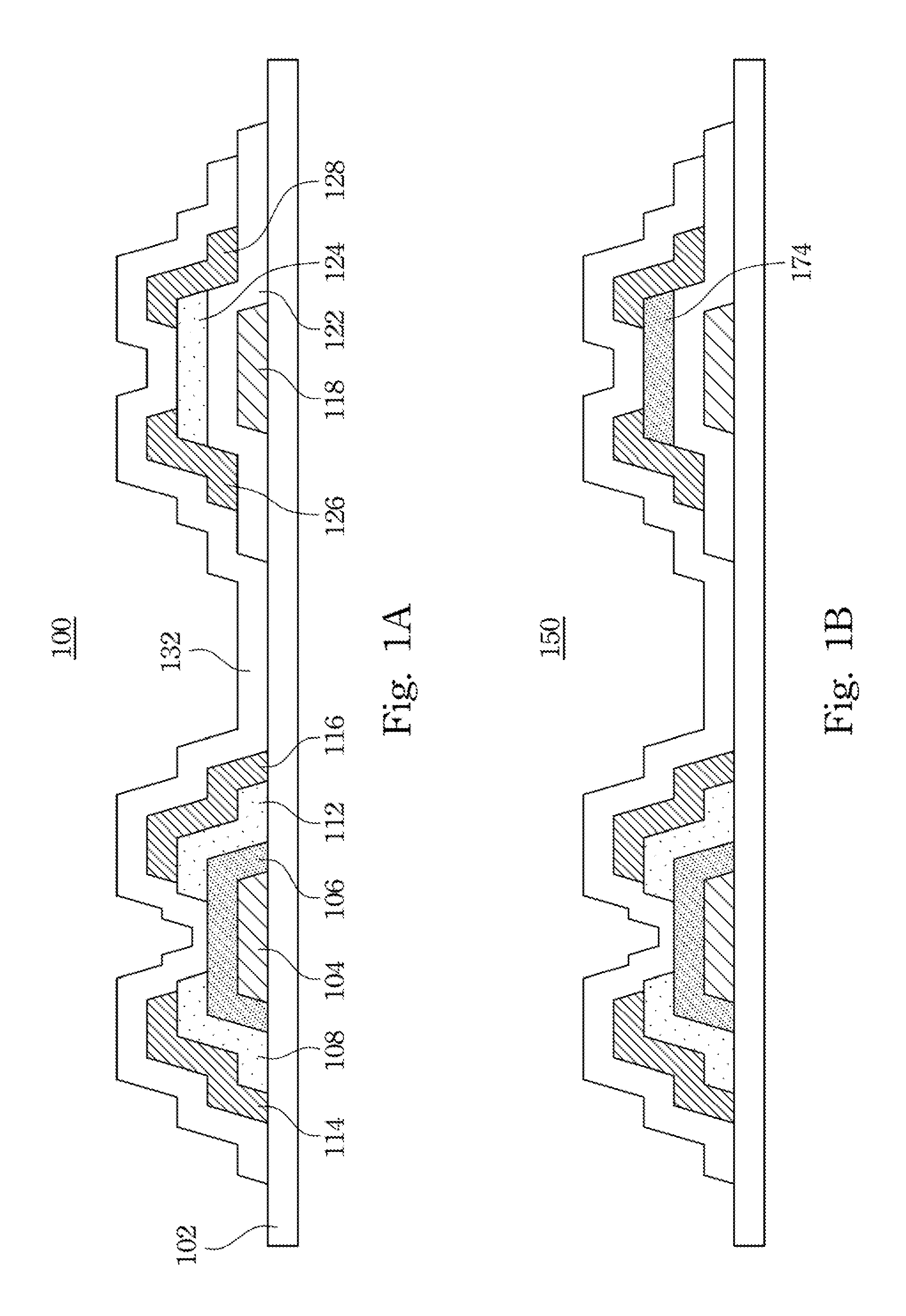
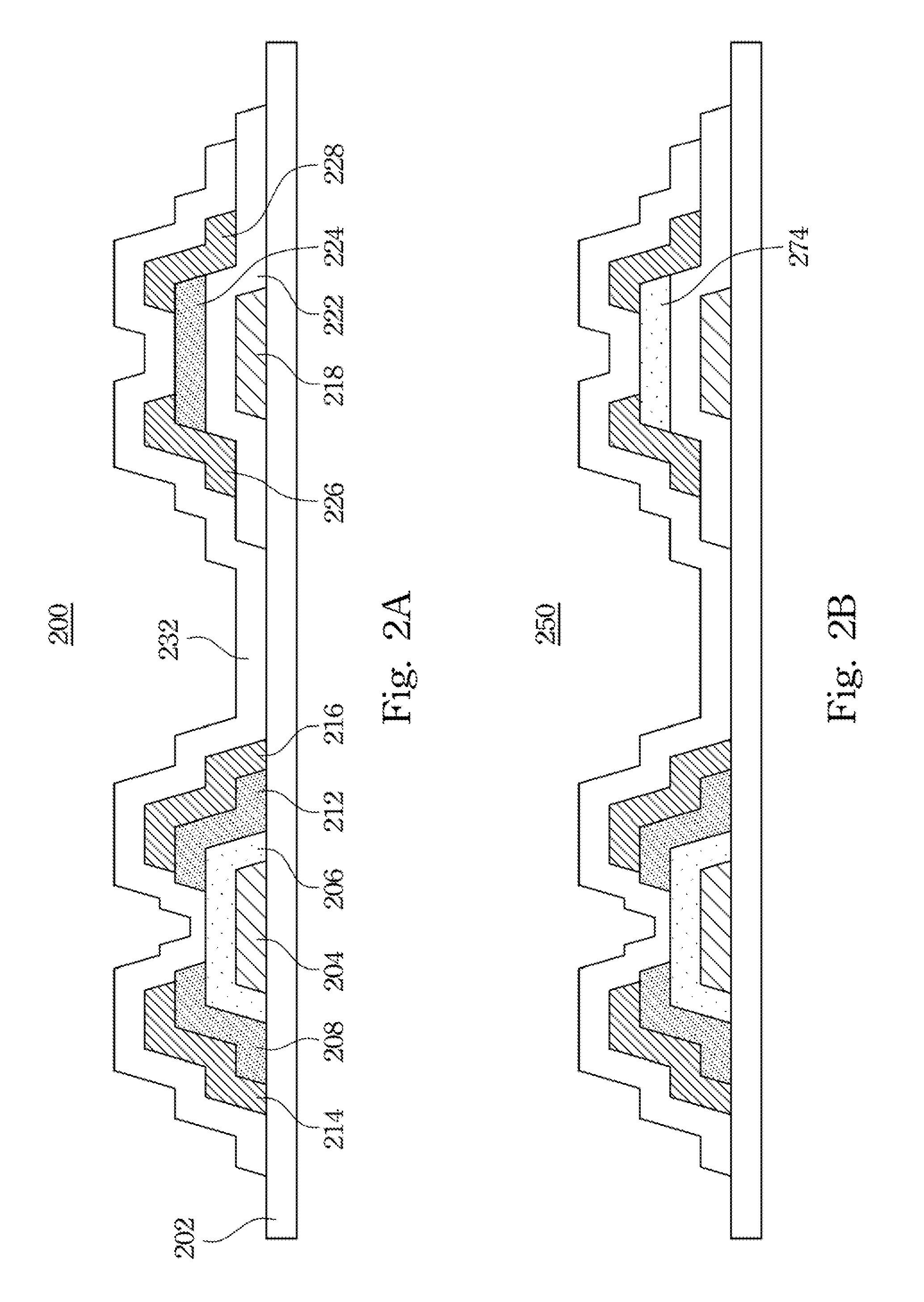
[0043]FIG. 2A and FIG. 2B shows schematically a diagram of a transistor structure according to the present invention. As shown in FIG. 2A, the transistor structure 200 comprises a first patterned conductive layer, a second patterned conductive layer, a third patterned conductive layer, a patterned P-type organic polymer semiconductor layer 206, a patterned N-type transparent oxide semiconductor layer, a patterned gate insulation layer 222, an active layer 224, and a covering insulation layer 232.

[0044]The first patterned conductive layer is formed over a substrate 202, and the first patterned conductive layer comprises a first portion 204 and a second portion 218, wherein the first portion 204 of the first patterned conductive layer is used as a base conductive layer (base electrode), the second portion 218 of the first patterned conductive layer is used as a gate. The patterned P-type organic polymer semiconductor layer 206 is formed on the first portion 204 of the first patterned ...

third embodiment

[0050]FIG. 3A and FIG. 3B shows schematically a diagram of a transistor structure according to the present invention. As shown in FIG. 3A, comparing with the transistor structure 100 as shown in FIG. 1A, the transistor structure 300 further comprises an insulation layer. The insulation layer is formed between the first portion 304 of the first patterned conductive layer and the patterned N-type transparent oxide semiconductor layer 306, and the insulation layer comprises a first portion 342 and a second portion 344, wherein the first portion 342 of the insulation layer is formed on one side of the first portion 304 of the first patterned conductive layer and the patterned N-type transparent oxide semiconductor layer 306. The second portion 344 of the insulation layer is formed on the other side of the first portion 304 of the first patterned conductive layer and the patterned N-type transparent oxide semiconductor layer 306. The insulation layer and the patterned gate insulation lay...

fifth embodiment

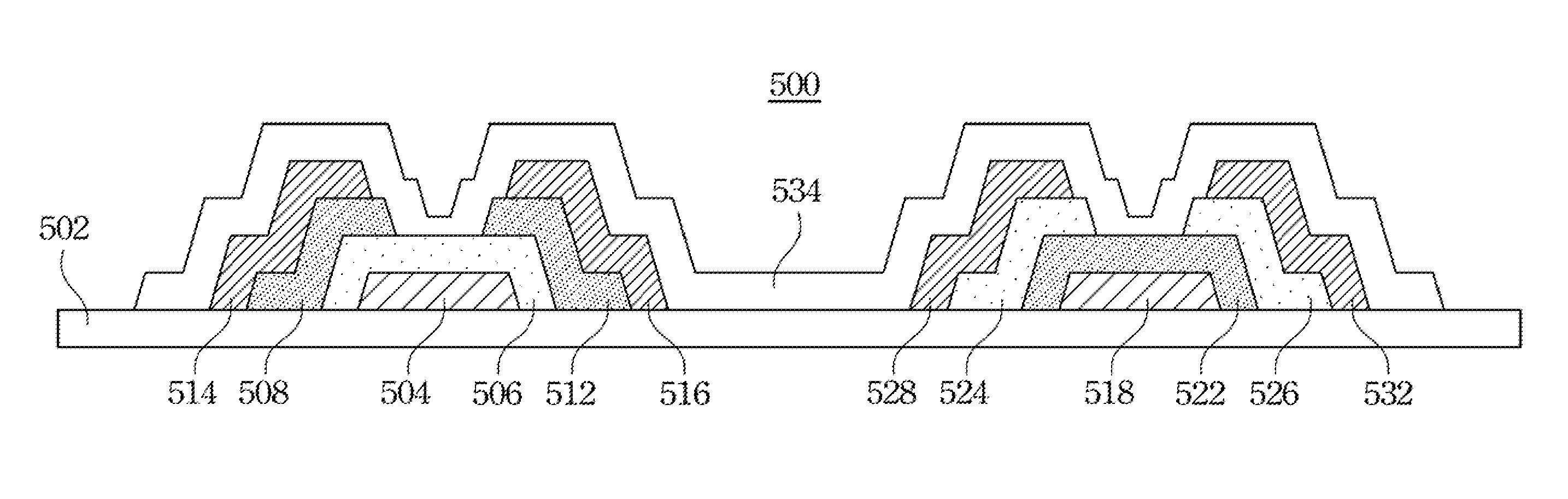
[0054]FIG. 5A and FIG. 5B shows schematically a diagram of a transistor to structure according to the present invention. As shown in FIG. 5A, a transistor structure 500 comprises a first patterned conductive layer, a second patterned conductive layer, a third patterned conductive layer, a first patterned P-type organic polymer semiconductor layer 506, a first patterned. N-type transparent oxide semiconductor layer, a second patterned N-type transparent oxide semiconductor layer 522, a second patterned P-type organic polymer semiconductor layer and a covering insulation layer 534.

[0055]The first patterned conductive layer is formed over a substrate 502, and the first patterned conductive layer comprises a first portion 504 and a second portion 518, wherein the first portion 504 of the first patterned conductive layer is used as a first base conductive layer (first base electrode), the second portion 518 of the first patterned conductive layer is used as a second base conductive layer...


PUM


Abstract

A transistor structure comprises a patterned N-type transparent oxide semiconductor formed over a substrate as a base, and a patterned p-type organic polymer semiconductor formed on the patterned N-type transparent oxide semiconductor comprising a first portion and a second portion so that the patterned N-type transparent oxide semiconductor and the first portion and the second portion of the patterned p-type organic polymer semiconductor form heterojunctions therebetween respectively, wherein the first portion of the patterned p-type organic polymer semiconductor is used as an emitter, and the second portion of the patterned p-type organic polymer semiconductor is used as a collector.

Description

RELATED APPLICATIONS[0001]This application claims priority to Taiwan Application Serial Number 099131063, filed Sep. 14, 2010, which is herein incorporated by reference.BACKGROUND[0002]1. Field of Invention[0003]The embodiment of the present invention relates generally to a transistor structure and, more particularly, to a transistor structure with transparent oxide semiconductor and organic polymer semiconductor.[0004]2. Description of Related Art[0005]Due to the development of the technology and the demand of the display quality by consumers, the technology of the display is mature day by day. The next generation display technology has been developed during recent years so that the display element is thinner, transparent, and flexible in the next generation display technology, and the quality and the property of the display element are the main research objective for the display.[0006]Conventionally, a-Si:H TFTs have been widely used in many applications. However, the process temp...

Claims


Application Information

Patent Timeline
Patent Type & Authority Patents(United States)
IPC IPC(8): H01L51/10
CPCH01L51/0096H01L27/286H01L27/283Y02E10/549Y02P70/50H10K19/20H10K19/10H10K77/10
Inventor YEH, CHIA-CHUNWANG, HENRYTSAI, YAO-CHOUHUANG, SUNG-HUI
Owner E INK HLDG INC
Why Eureka
Try Eureka