Semiconductor device accommodating semiconductor module with heat radiation structure

a technology of semiconductor modules and semiconductor devices, applied in semiconductor devices, lighting and heating apparatus, cooling/ventilation/heating modifications, etc., can solve problems such as restricted thermal design, and achieve the effect of effective cooling

Active Publication Date: 2013-01-29
DENSO CORP
View PDF15 Cites 17 Cited by
  • Summary
  • Abstract
  • Description
  • Claims
  • Application Information

AI Technical Summary

Benefits of technology

[0008]An embodiment provides a semiconductor device including a semiconductor module in which semiconductor chips, each in which a semiconductor power element is formed, are disposed in alignment upstream and downstream of a coolant flow, the semiconductor device in which the rise in semiconductor chip temperature on the downstream side to a temperature higher than that on the upstream side can be suppressed, and the semiconductor chips disposed upstream and downstream can be more effectively cooled.
[0010]In this way, of the upper arm and the lower arm, the arm having the greater thermal resistance is positioned upstream of the coolant flow, and the arm having the smaller thermal resistance is positioned downstream of the coolant flow. Therefore, the first and second semiconductor chips disposed upstream and downstream can be effectively cooled by the rise in coolant temperature on the upstream side being suppressed. Alternatively, even when the coolant temperature rises on the upstream side, the first and second semiconductor chips disposed upstream and downstream can be effectively cooled by sufficient cooling being performed on the downstream side based on the high cooling efficiency.
[0011]Thus, in the semiconductor device including the semiconductor module in which the first and second semiconductor chips, each in which a semiconductor power element is formed, are disposed in alignment upstream and downstream of the coolant flow, the rise in semiconductor chip temperature on the downstream side to a temperature higher than that on the upstream side can be suppressed. As a result, the first and second semiconductor chips disposed upstream and downstream can be more effectively cooled.
[0013]In this instance, when the third heat sink is of a size longer than the size of the first heat sink in the array direction of the upper arm and the lower arm, the cooling efficiency of the lower arm disposed further downstream of the coolant flow can be increased. Therefore, the above-described effects can be further effectively achieved.

Problems solved by technology

Therefore, thermal design is restricted by the semiconductor power element on the downstream side in which temperature rise occurs.

Method used


Image

  • Semiconductor device accommodating semiconductor module with heat radiation structure
  • Semiconductor device accommodating semiconductor module with heat radiation structure
  • Semiconductor device accommodating semiconductor module with heat radiation structure

Examples


first embodiment

[0034]A first embodiment of the present invention will be described. According to the first embodiment, a semiconductor device including a semiconductor module according to an embodiment of the present invention will be described, giving as an example an inverter having a cooling mechanism.

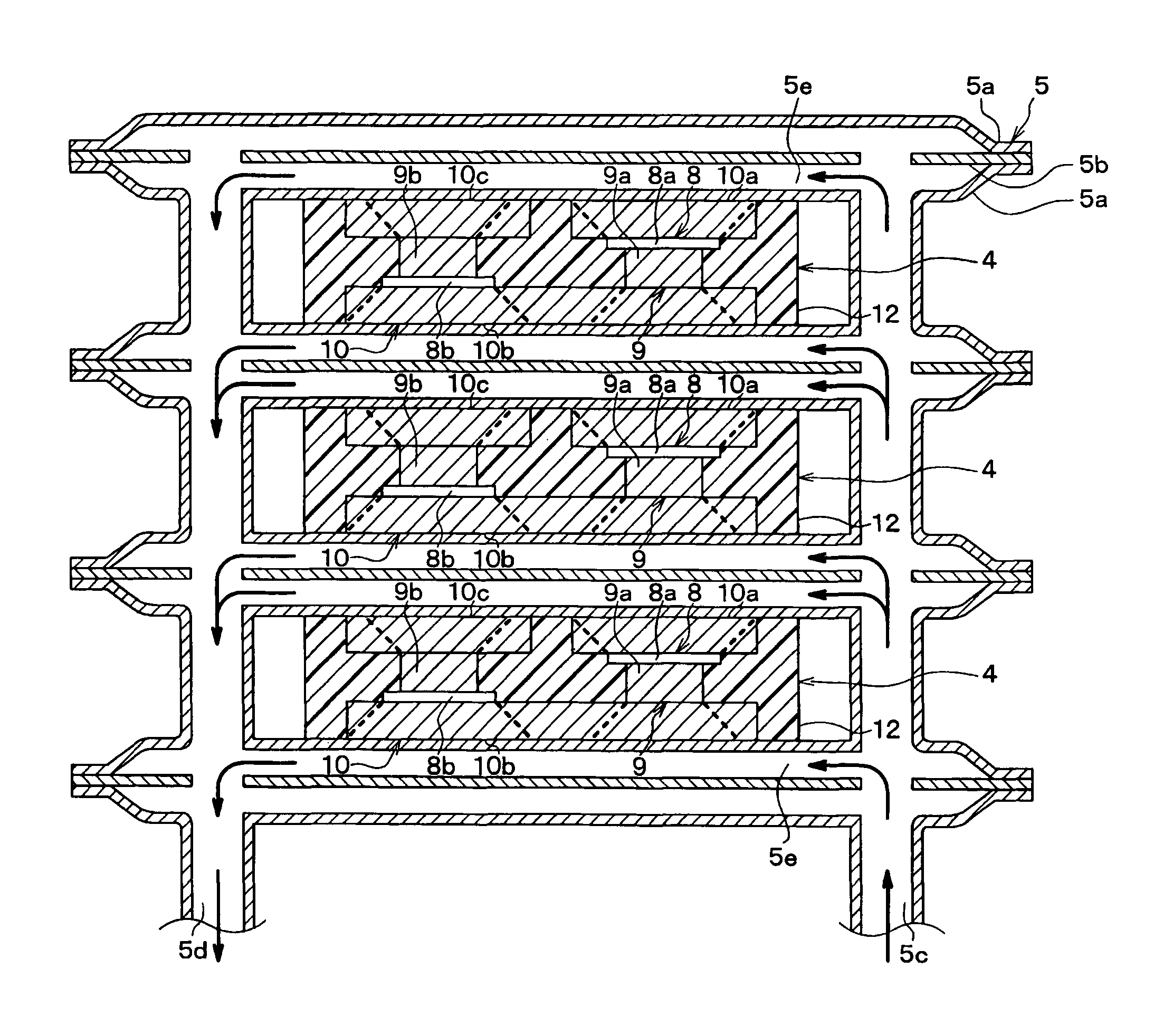
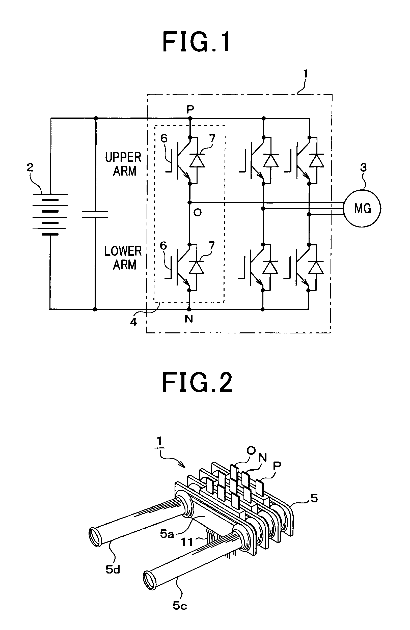
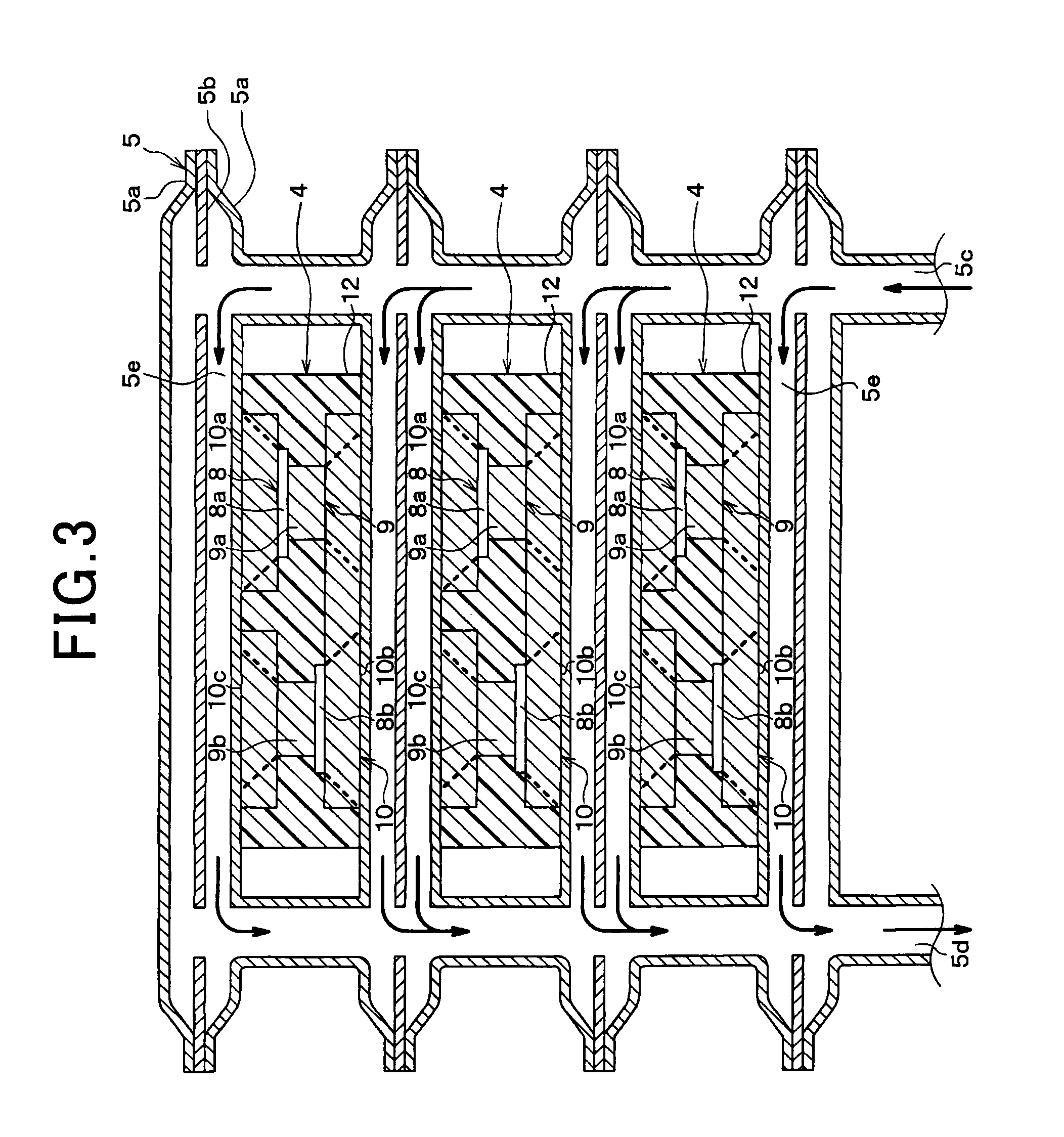
[0035]FIG. 1 is a circuit diagram of an inverter 1. FIG. 2 is a perspective view of the inverter 1. FIG. 3 is a cross-sectional view of the inverter 1. FIG. 3 is equivalent to a cross-section of the inverter 1 taken on a plane perpendicular to the up / down direction of the surface of the paper on which FIG. 2 is printed.

[0036]As shown in FIG. 1, the inverter 1 is used to drive, with an alternating current, a three-phase motor 3 that is a load, based on a direct-current power supply 2. The inverter 1 is configured such that serially connected upper arms and lower arms are connected in parallel in three phases. An intermediate potential of the upper arm and the lower arm is applied while being sequen...

second embodiment

[0064]A second embodiment of the present invention will be described. According to the second embodiment, the structure of the semiconductor module 4 is changed from that according to the first embodiment. Other aspects are similar to those according to the first embodiment and, therefore, only sections that differ will be described.

[0065]FIG. 9 is a cross-sectional view of the semiconductor module 4 according to the second embodiment. As shown in FIG. 9, the semiconductor module 4 according to the second embodiment basically has a similar structure as that according to first embodiment, aside from the sizes of the heat sinks 10a and 10c being changed from those according to the first embodiment. Specifically, the size of the heat sink 10c is greater than the size of the heat sink 10a in the left / right direction of the surface of the paper on which FIG. 9 is printed.

[0066]As a result of a structure such as this, the thermal resistance R2 of the lower arm disposed further downstream ...

third embodiment

[0067]A third embodiment of the present invention will be described. According to the third embodiment, the structure of the semiconductor module 4 is changed from that according to the first embodiment. Other aspects are similar to those according to the first embodiment and, therefore, only sections that differ will be described.

[0068]FIG. 10 is a cross-sectional view of the semiconductor module 4 according to the third embodiment. As shown in FIG. 10, the semiconductor module 4 according to the third embodiment basically has a similar structure as that according to first embodiment, aside from the semiconductor module 4 being assembled in the cooling mechanism 5 such that the lower arm is disposed on the upstream side of the coolant flow in the cooling mechanism 5 and the upper arm is disposed on the downstream side. The width of the heat sink 10a of the upper arm becomes wider compared to that of the heat sink 10b of the lower arm disposed on the upper stream side, in the left / r...


PUM


Abstract

As a result of a lower arm side having a small thermal resistance being positioned downstream of the coolant flow, cooling efficiency of the lower arm positioned on the downstream side of the coolant flow becomes higher than that of an upper arm positioned on an upstream side. Hence, rise in coolant temperature on the upstream side can be suppressed, and the first and second semiconductor chips disposed upstream and downstream can be effectively cooled. Alternatively, even when the coolant temperature rises on the upstream side, the first and second semiconductor chips disposed upstream and downstream can be effectively cooled by sufficient cooling being performed on the downstream side based on the high cooling efficiency. Therefore, the rise in semiconductor chip temperature on the downstream side to a temperature higher than that on the upstream side can be suppressed.

Description

CROSS REFERENCE TO RELATED APPLICATION[0001]This application is based on and claims the benefit of priority from earlier Japanese Patent Application Numbers 2010-78256 filed on Mar. 30, 2010 and 2011-28680 filed on Feb. 14, 2011 the description of which is incorporated herein by reference.BACKGROUND[0002]1. Technical Field[0003]The present invention relates to a semiconductor device including a semiconductor module in which a semiconductor chip and a heat sink are sealed by a resin to form an integrated structure, the semiconductor chip in which a semiconductor power element is formed of which heat radiation is performed by the heat sink. The present invention is suitably applied to a semiconductor device including a semiconductor module having, for example, a two-in-one structure in which two semiconductor power elements of an upper arm (high-side element) and a lower arm (low-side element) are sealed in a single resin sealing section.[0004]2. Description of the Related Art[0005]Co...

Claims


Application Information

Patent Timeline
Patent Type & Authority Patents(United States)
IPC IPC(8): H05K7/20F28F7/00H01L23/34
CPCH01L23/4334H01L23/473H01L25/072H01L25/117H01L2224/291H01L2924/13055H01L2224/33181H01L2224/32245H01L2924/1305H01L2924/13091H01L2924/014H01L2924/00H01L23/4012
Inventor TONOMOTO, MASAYA
Owner DENSO CORP
Why Eureka
Try Eureka