Semiconductor device including a Trench-Gate Fin-FET
a technology of trench gate fin and field effect transistor, which is applied in the direction of semiconductor devices, transistors, electrical devices, etc., can solve the problems of sub-threshold voltage characteristics deteriorating and the threshold voltage becomes lower, so as to increase contact resistance, reduce on-current, and widen the active region.
- Summary
- Abstract
- Description
- Claims
- Application Information
AI Technical Summary
Benefits of technology
Problems solved by technology
Method used
Image
Examples
first exemplary embodiment
[0026]In a first exemplary embodiment, a semiconductor device as the Trench-Gate Fin-FET is set forth in which the width of the active region is 60 nm and the width of the channel region is 30 nm.
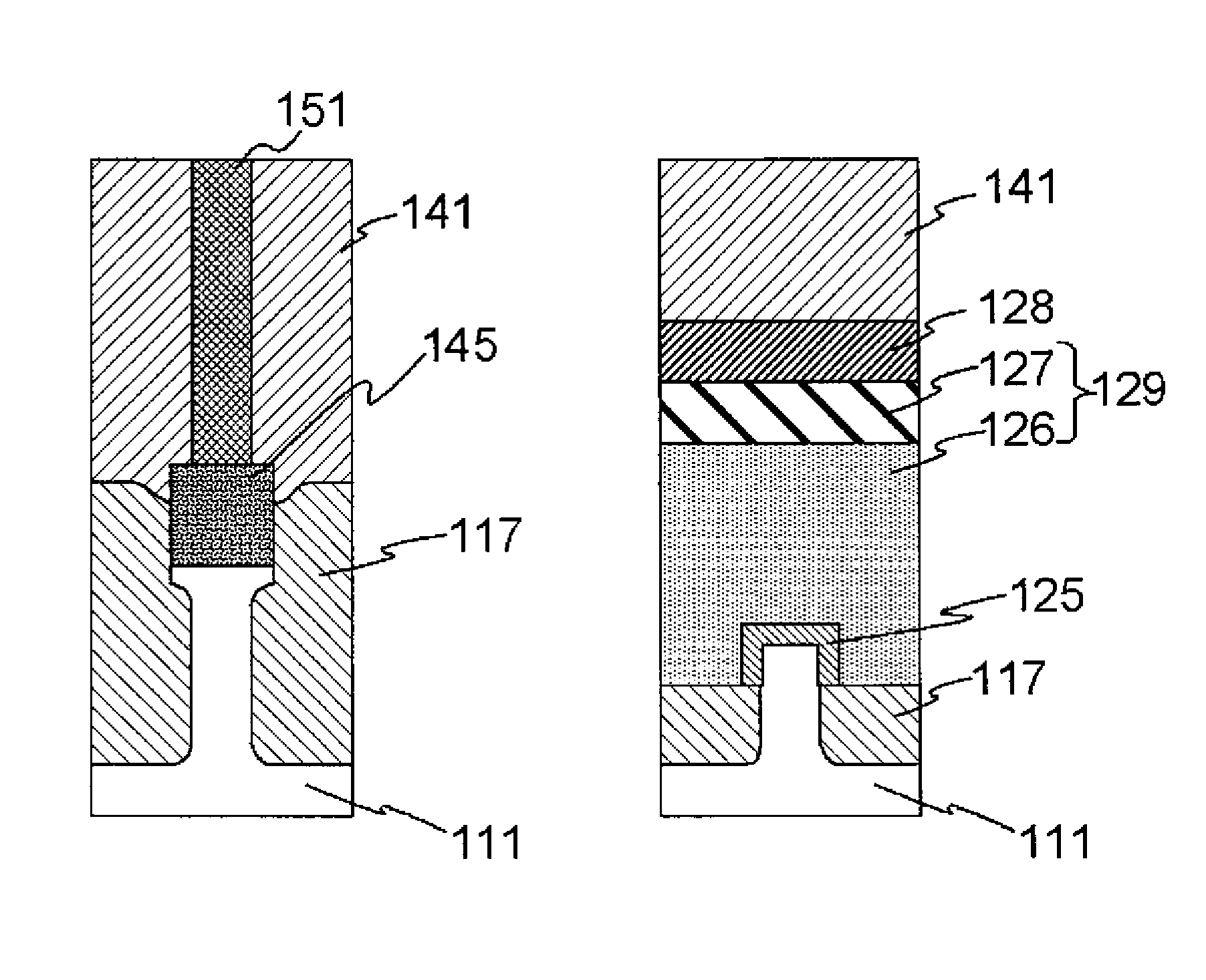
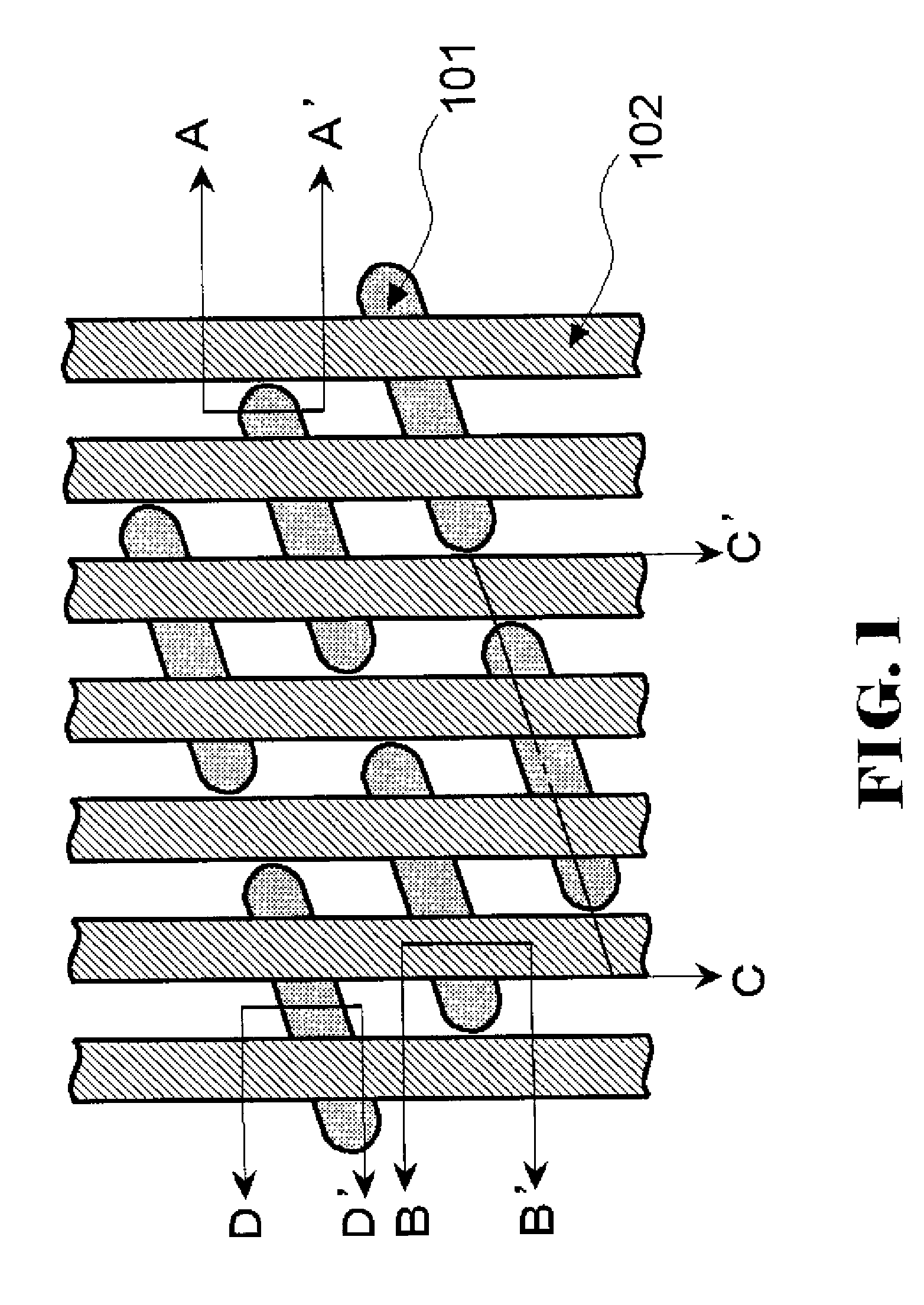
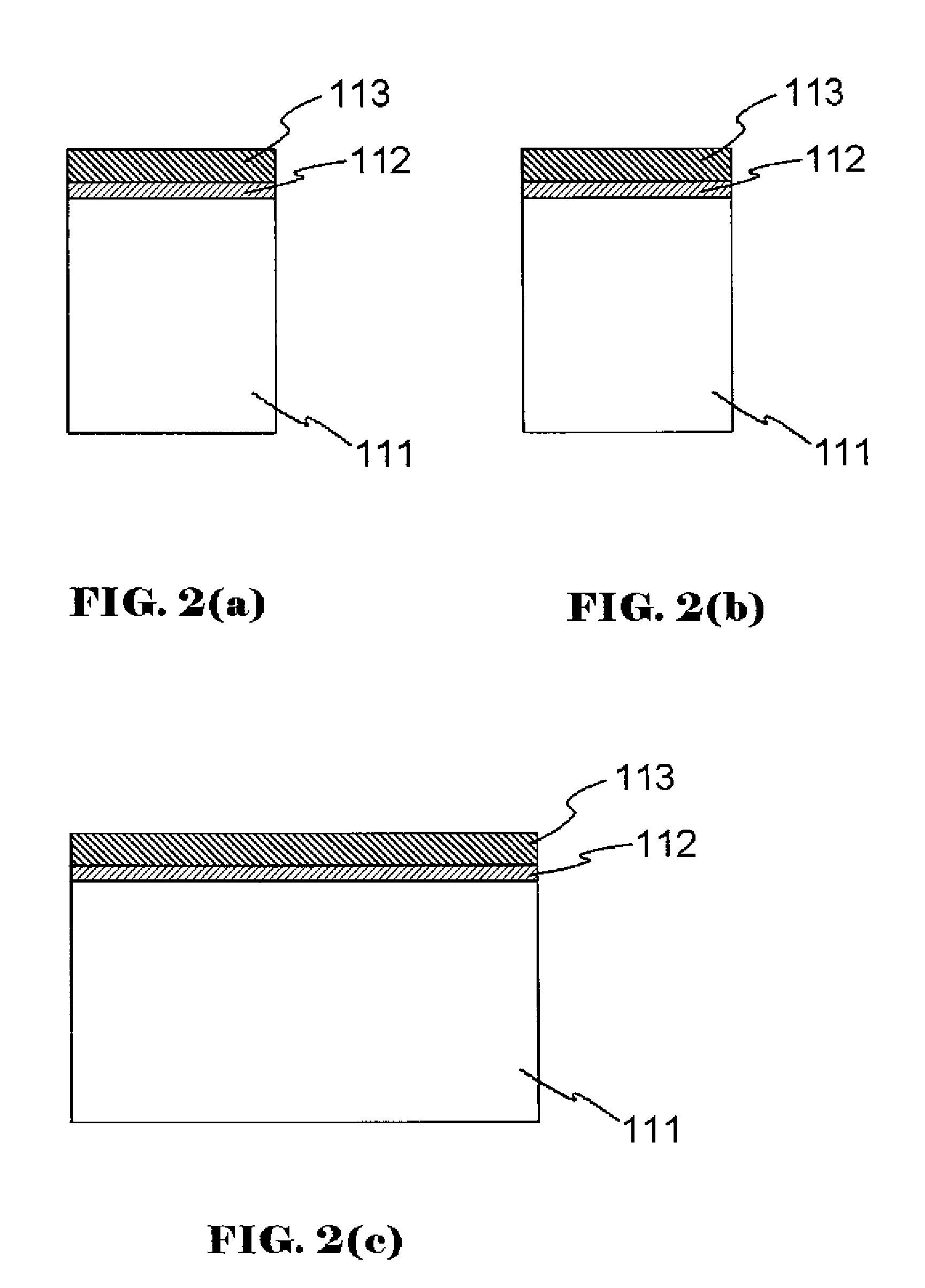
[0027]In the first exemplary embodiment, an example is described referring to the figures in which the present invention, i.e., the semiconductor device is used as a memory cell transistor of DRAM including n-MOS-FET structure. FIG. 1 is a plan view showing a portion of a memory cell region of the DRAM according to an exemplary embodiment of the present invention. FIG. 2 to FIG. 8, FIG. 10 to FIG. 12, and FIG. 14 to FIG. 21 are cross-sectional views of processes showing manufacturing processes according to the first exemplary embodiment of the present invention; FIG. 9 is a cross-sectional view of a process showing a manufacturing process according to a variant of the first exemplary embodiment; and in which figures (a) and (b) show cross-sections of the Trench-Gate Fin-FET of FIG. 1 taken ...
second exemplary embodiment
[0058]In a second exemplary embodiment, a semiconductor device as Embedded-Gate Fin-FET having an embedded gate which is one kind of the trench gate is set forth in which the width of the active region is 60 nm and the width of the channel region is 30 nm.
[0059]In the second exemplary embodiment, an example in which the Embedded-Gate Fin-FET is used as a memory cell transistor of DRAM is described referring to the drawings. Firstly, in the same way as the first exemplary embodiment, the processes as shown in FIG. 2 to FIG. 10 are executed. In the meanwhile, silicon substrate 111 is etched away by a depth of 100 nm in FIG. 4 as in the first exemplary embodiment and, further, silicon substrate 111 is etched away by a depth larger than a depth of source and drain diffusion layers to be connected to a capacitor of the DRAM.
[0060]Thereafter, as shown in FIG. 26, silicon nitride film 113 is removed using hot phosphoric acid. Next, source and drain diffusion layers 219 are formed with a ju...
PUM
 Abstract
Description
Claims
Application Information


