Semiconductor device

a technology of semiconductors and devices, applied in the direction of semiconductor devices, electrical equipment, transistors, etc., can solve the problems of sub-threshold voltage characteristics deterioration and lower threshold voltage, and achieve the effects of increasing contact resistance, reducing on-current, and widening the active region

Inactive Publication Date: 2011-03-03
PS4 LUXCO SARL
View PDF5 Cites 39 Cited by
  • Summary
  • Abstract
  • Description
  • Claims
  • Application Information

AI Technical Summary

Benefits of technology

[0010]According to an exemplary embodiment of the present invention, in the Trench-Gate Fin-FET, by making the fin width of the channel region relative to an effective channel length smaller, the advantage which shall be exerted in the Fin-FET can be sufficiently taken even if the transistor becomes finer. At the same time, because the width of the active region can be larger than the width of the channel region, the decreasing of the on-current due to the increasing of the contact resistance following the miniaturization of the transistor can be suppressed.

Problems solved by technology

Recently, with a miniaturization of a transistor, it is being problematic that due to a so-called short channel effect, threshold voltage becomes lower and sub-threshold voltage characteristic becomes deteriorated.

Method used


Image

  • Semiconductor device
  • Semiconductor device
  • Semiconductor device

Examples


first exemplary embodiment

[0026]In a first exemplary embodiment, a semiconductor device as the Trench-Gate Fin-FET is set forth in which the width of the active region is 60 nm and the width of the channel region is 30 nm.

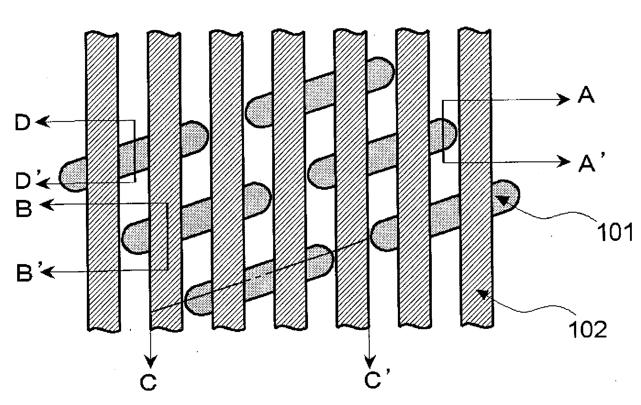
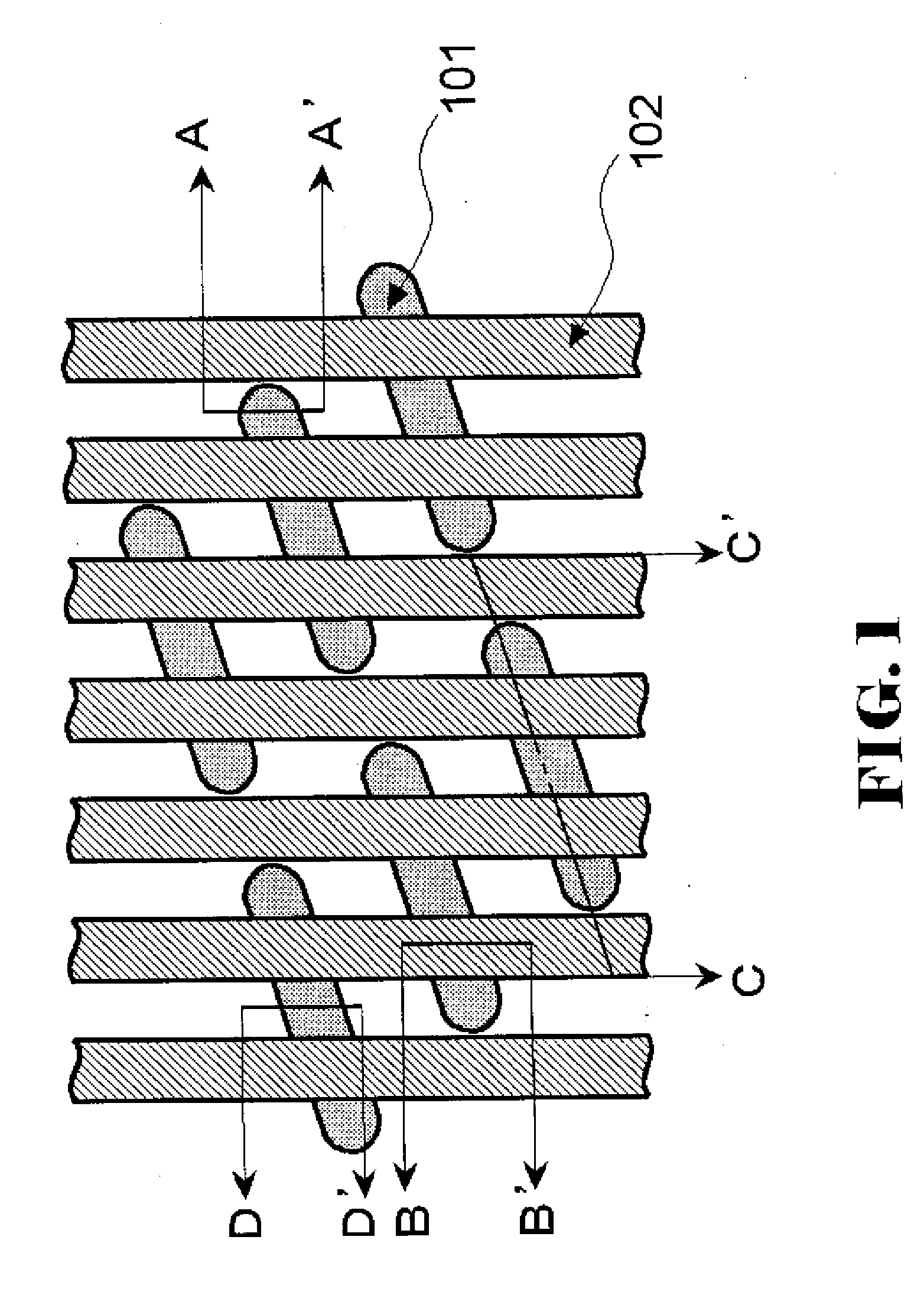
[0027]In the first exemplary embodiment, an example is described referring to the figures in which the present invention, i.e., the semiconductor device is used as a memory cell transistor of DRAM including n-MOS-FET structure. FIG. 1 is a plan view showing a portion of a memory cell region of the DRAM according to an exemplary embodiment of the present invention. FIG. 2 to FIG. 8, FIG. 10 to FIG. 12, and FIG. 14 to FIG. 21 are cross-sectional views of processes showing manufacturing processes according to the first exemplary embodiment of the present invention; FIG. 9 is a cross-sectional view of a process showing a manufacturing process according to a variant of the first exemplary embodiment; and in which figures (a) and (b) show cross-sections of the Trench-Gate Fin-FET of FIG. 1 taken ...

second exemplary embodiment

[0055]In a second exemplary embodiment, a semiconductor device as Embedded-Gate Fin-FET having an embedded gate which is one kind of the trench gate is set forth in which the width of the active region is 60 nm and the width of the channel region is 30 nm.

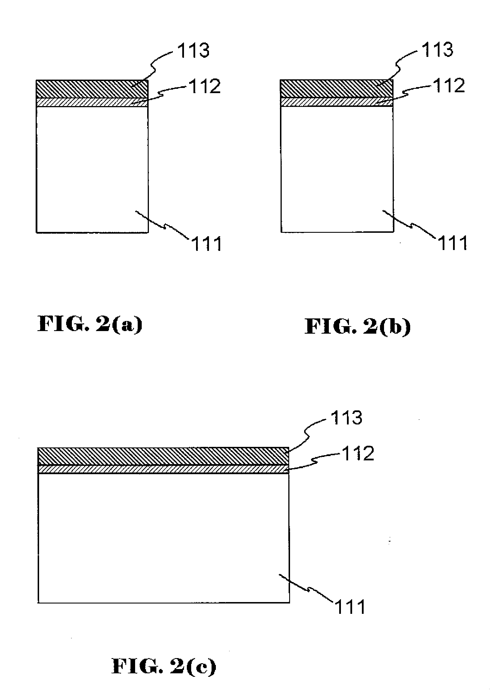
[0056]In the second exemplary embodiment, an example in which the Embedded-Gate Fin-FET is used as a memory cell transistor of DRAM is described referring to the drawings. Firstly, in the same way as the first exemplary embodiment, the processes as shown in FIG. 2 to FIG. 10 are executed. In the meanwhile, silicon substrate 111 is etched away by a depth of 100 nm in FIG. 4 as in the first exemplary embodiment and, further, silicon substrate 111 is etched away by a depth larger than a depth of source and drain diffusion layers to be connected to a capacitor of the DRAM.

[0057]Thereafter, as shown in FIG. 26, silicon nitride film 113 is removed using hot phosphoric acid. Next, source and drain diffusion layers 219 are formed with a ju...


PUM


Abstract

In Trench-Gate Fin-FET, in order that the advantage which is exerted in Fin-FET can be sufficiently taken even if a transistor becomes finer and, at the same time, decreasing of on-current can be suppressed by saving a sufficiently large contact area in the active region, a fin width 162 of a channel region becomes smaller than a width 161 of an active region.

Description

BACKGROUND OF THE INVENTION[0001]1. Field of the Invention[0002]The present invention relates to a semiconductor device, and more particularly to a semiconductor device including a trench gate fin field effect transistor (Trench-Gate Fin-FET).[0003]2. Description of the Related Art[0004]Recently, with a miniaturization of a transistor, it is being problematic that due to a so-called short channel effect, threshold voltage becomes lower and sub-threshold voltage characteristic becomes deteriorated. As a high-performance transistor suppressing such a problem, a fin field effect transistor (Fin-FET) has been remarked whose channel is fabricated in fin shape. Further, in order to use the Fin-FET as a transistor with a low leakage requirement such as a cell transistor of a dynamic random access memory (DRAM), Trench-Gate Fin-FET (also called as a saddle Fin-FET) is set forth which combines a trench gate structure with the fin structure (Japanese Patent Laid-Open No. 2008-47909, Japanese ...

Claims


Application Information

Patent Timeline
Patent Type & Authority Applications(United States)
IPC IPC(8): H01L27/108H01L27/06
CPCH01L21/823431H01L27/10823H01L29/785H01L27/10879H01L29/66818H01L27/10876H10B12/34H10B12/056H10B12/053
Inventor TAKETANI, HIROAKI
Owner PS4 LUXCO SARL
Why Eureka
Try Eureka