
Device for and a method of processing data signals

a data signal and device technology, applied in the direction of digital transmission, pulse technique, electrical apparatus, etc., can solve the problems of poor chip, reduced yield, heavy use of calibration techniques and digital signal processing, etc., and achieve the effect of improving raw image rejection

Inactive Publication Date: 2013-02-12
NXP BV
View PDF11 Cites 0 Cited by
  • Summary
  • Abstract
  • Description
  • Claims
  • Application Information

AI Technical Summary

Benefits of technology

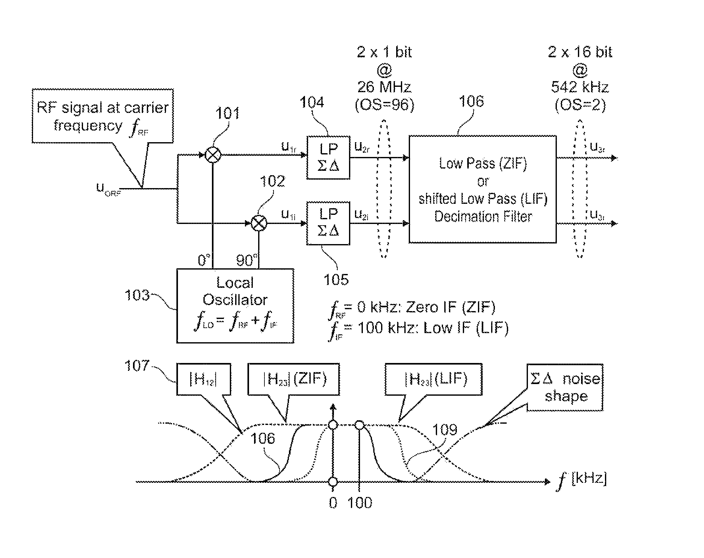
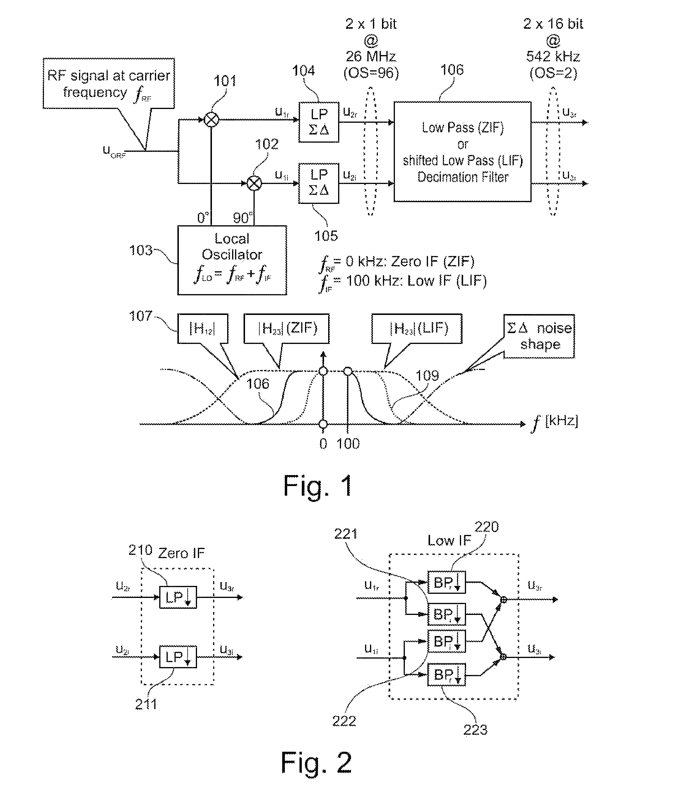
[0008]It is an object of the invention to provide a data signal processing device and a data signal processing method which can be used to improve raw image rejection in a Low IF receiver, in particular by using digital processing.
[0015]By using a rectangular filtering matrix it may be possible to provide an efficient image rejection in a Low IF receiver, in particular by using digital processing. That is, it may be possible to efficiently cancel images generated in case of asymmetries in the analogue part of the filtering device, which images are hard to correct in the digital domain when using a conventional digital filtering system.
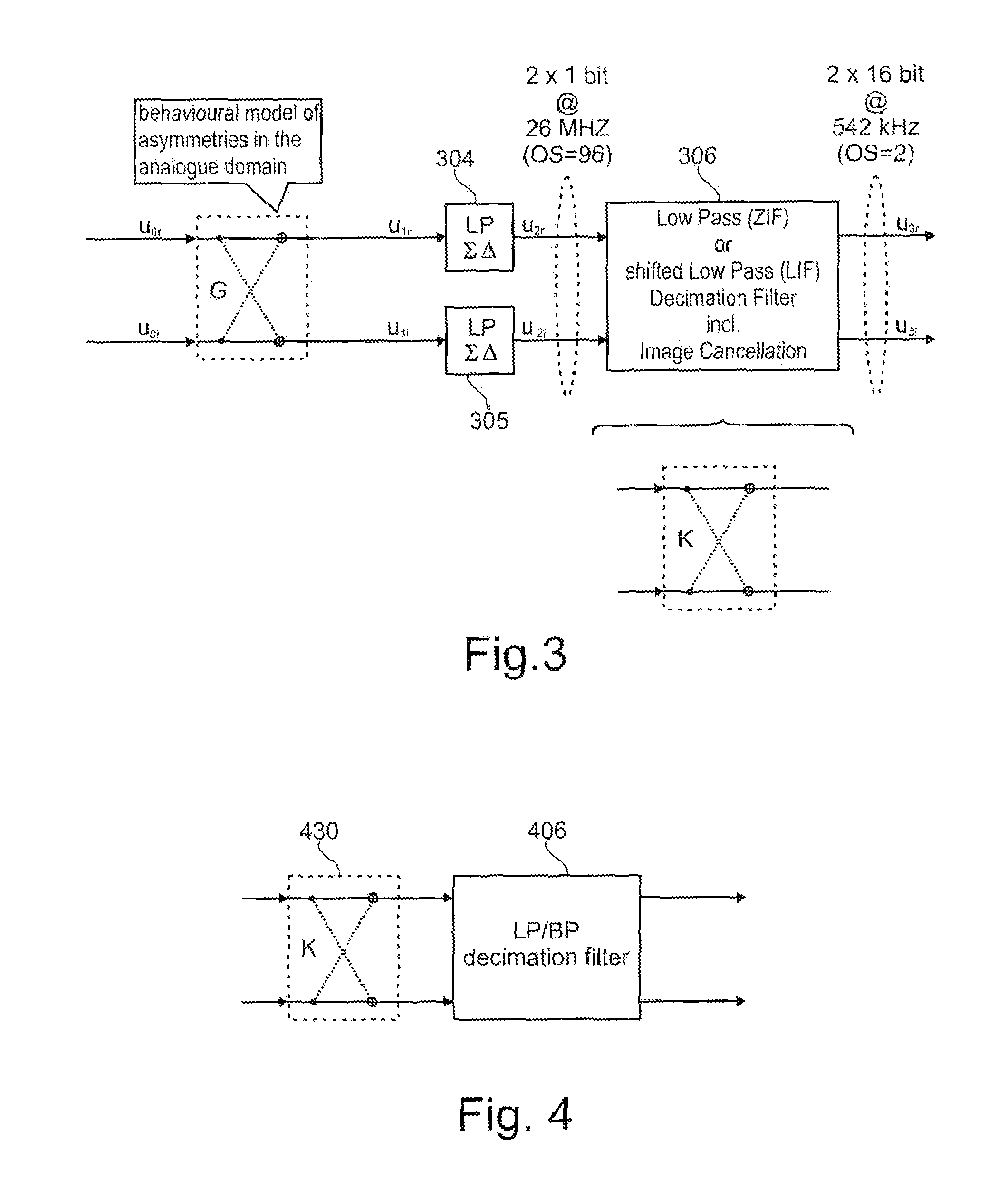
[0028]An exemplary aspect of the invention may be seen in providing a method of image cancellation including the multiplying of a digital data signal by a matrix in the digital domain, wherein the matrix multiplying is performed after a pre-filtering, e.g. a decimation filtering, and using a rectangular matrix, e.g. a 2×4 matrix. The digital data signal may be a quadrature signal. The using of a rectangular matrix may particularly ensure that known advantages of a Zero IF solution may also be achievable in a Low IF case. In particular, the filtering or image cancellation may be merged with decimation filtering in sigma delta type ADCs, which may result in a very efficient implementation that preserves the advantages of decimation filters for low resolution input. The provided method may not be restricted to certain wireless communication standards but may be generic. By implementing the matrix multiplying, which builds an image cancellation (IC) block, after the decimation filter it may be possible to reuse efficient decimation filter designs for 1 bit input instead of developing a complicate redesign of the DF. Furthermore, the usage of a method according to an exemplary embodiment may omit the necessary to perform the IC filtering or function at high sampling rate.

Problems solved by technology

If one of the figures of merits of a given chip is outside the specified range, then this chip is bad and reduces the yield.
This leads to heavy use of calibration techniques and digital signal processing.
With the switch to CMOS technology, these problems recurred and / or new problems came up, with the consequence that some manufacturers have changed from Zero IF to Low IF in their 2.5G cellular products.

Method used


Image

  • Device for and a method of processing data signals
  • Device for and a method of processing data signals
  • Device for and a method of processing data signals

Examples


case 1

[0060] IC prior to DF

[0061]case 2: single stage DF with post IC

case 3

[0062] double stage DF with post IC

case 4

[0063] double stage DF with intermediate IC.

[0064]The IC functions employ the 2-by-2 matrix K or the 2-by-4 matrix M.

[0065]The matrix multiply block in the following block diagrams visualizes the order of magnitude of the respective matrix elements in K and M: A solid branch indicates a weight of approximately 1.0 and a dotted branch indicates a weight of approximately 0. When symmetry in the analogue part of the receiver is perfect and IC is not required, the weights become exactly 1.0 and 0.

[0066]FIG. 4 depicts the case of IC prior to DF. This brute force approach corresponds to the implementation of a multiplication of the data signal by the matrix K 430, i.e. the image cancellation, before the decimation filter 406 which is a less preferred embodiment because of 2 reasons: First, the output of the IC block must be multi bit in order to keep the pass band clean of quantisation noise. This complicates the design of the DF which can not take advantage of a 1 bit input signal any mo...


PUM


Abstract

A method of data signal processing is provided, wherein the method comprises filtering a pre-filtered quadrature data signal by using an m×n filtering matrix, wherein m≠n. In particular, the filtering may be performed by using a rectangular matrix, i.e. a non-quadratic matrix. That is, the filtering may be performed by a matrix multiply in an image cancellation filtering unit. In general m relates to the 5 number of rows of the matrix while n relates to the number of columns of the matrix. In particular, the processing may form or may be a part of an image cancellation process.

Description

FIELD OF THE INVENTION[0001]The invention relates to a device for processing data signals, in particular for performing image cancellation of the data signals.[0002]The invention further relates to a method of processing data signals, in particular to an image cancellation method.[0003]Moreover, the invention relates to a program element. Further, the invention relates to a computer-readable medium.BACKGROUND OF THE INVENTION[0004]There is a trend in hand-held devices for mobile communications towards Systems on Chip (SoCs), meaning that the digital baseband (BB) sub system and the RF sub system are integrated on a single chip in CMOS technology. Traditionally, these two subsystems were implemented on dedicated chips in CMOS and BiCMOS technology, respectively. SoCs promise cost reduction, provided the high yield known from purely digital chips is reached:[0005]The RF subsystem is characterized by several figures of merit, such as image rejection or noise figure. If one of the figur...

Claims


Application Information

Patent Timeline
Patent Type & Authority Patents(United States)
IPC IPC(8): H04B1/10
CPCH04B1/30
Inventor BODE, PETER
Owner NXP BV
Learn More