Semiconductor device

a technology of semiconductor devices and semiconductors, applied in the direction of solid-state devices, transistors, instruments, etc., can solve the problem of extremely long data storage time, and achieve the effect of increasing the integration degree of semiconductor devices

Active Publication Date: 2013-02-19
SEMICON ENERGY LAB CO LTD
View PDF142 Cites 61 Cited by
  • Summary
  • Abstract
  • Description
  • Claims
  • Application Information

AI Technical Summary

Benefits of technology

[0010]In view of the above problems, an object of one embodiment of the present invention is to provide a semiconductor device with a novel structure in which stored data can be held even when power is not supplied and there is no limit on the number of write operations. Another object is to increase the integration degree of the semiconductor device with a novel structure.
[0011]In one embodiment of the present invention, a semiconductor device is manufactured using an oxide semiconductor. In particular, a highly purified oxide semiconductor is used. A transistor including an oxide semiconductor has extremely low leakage current; therefore, data can be held for a long time. In the case of using a highly purified oxide semiconductor, leakage current is much lower and thus data can be held for an extremely long time.
[0024]Since the off-state current of a transistor including an oxide semiconductor is extremely low, stored data can be held for a long time by using the transistor. In other words, power consumption can be sufficiently reduced because refresh operation becomes unnecessary or the frequency of refresh operation can be extremely low. Moreover, stored data can be held for a long time even when power is not supplied.
[0025]Further, a semiconductor device according to one embodiment of the present invention does not need high voltage for data writing, and there is no problem of deterioration of an element. For example, since there is no need to perforin injection of electrons into a floating gate and extraction of electrons from the floating gate which are needed in a conventional nonvolatile memory, deterioration of a gate insulating layer does not occur. That is, the semiconductor device according to one embodiment of the present invention does not have a limit on the number of times of rewriting, which has been a problem of a conventional nonvolatile memory, and thus has significantly improved reliability. Furthermore, data is written by turning on or off the transistor, whereby high-speed operation can be easily realized. In addition, there is an advantage in that operation for erasing data is not needed.
[0026]Since a transistor including a material other than an oxide semiconductor can operate at sufficiently high speed, a semiconductor device in which the transistor is used in combination with a transistor including an oxide semiconductor can perform operation (e.g., data reading) at sufficiently high speed. Further, with the transistor including a material other than an oxide semiconductor, a variety of circuits (such as a logic circuit or a driver circuit) which is required to operate at high speed can be favorably realized.

Problems solved by technology

In the case of using a highly purified oxide semiconductor, leakage current is much lower and thus data can be held for an extremely long time.

Method used


Image

  • Semiconductor device
  • Semiconductor device
  • Semiconductor device

Examples


embodiment 1

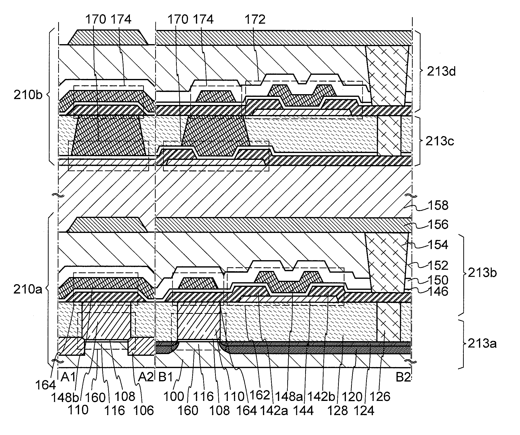
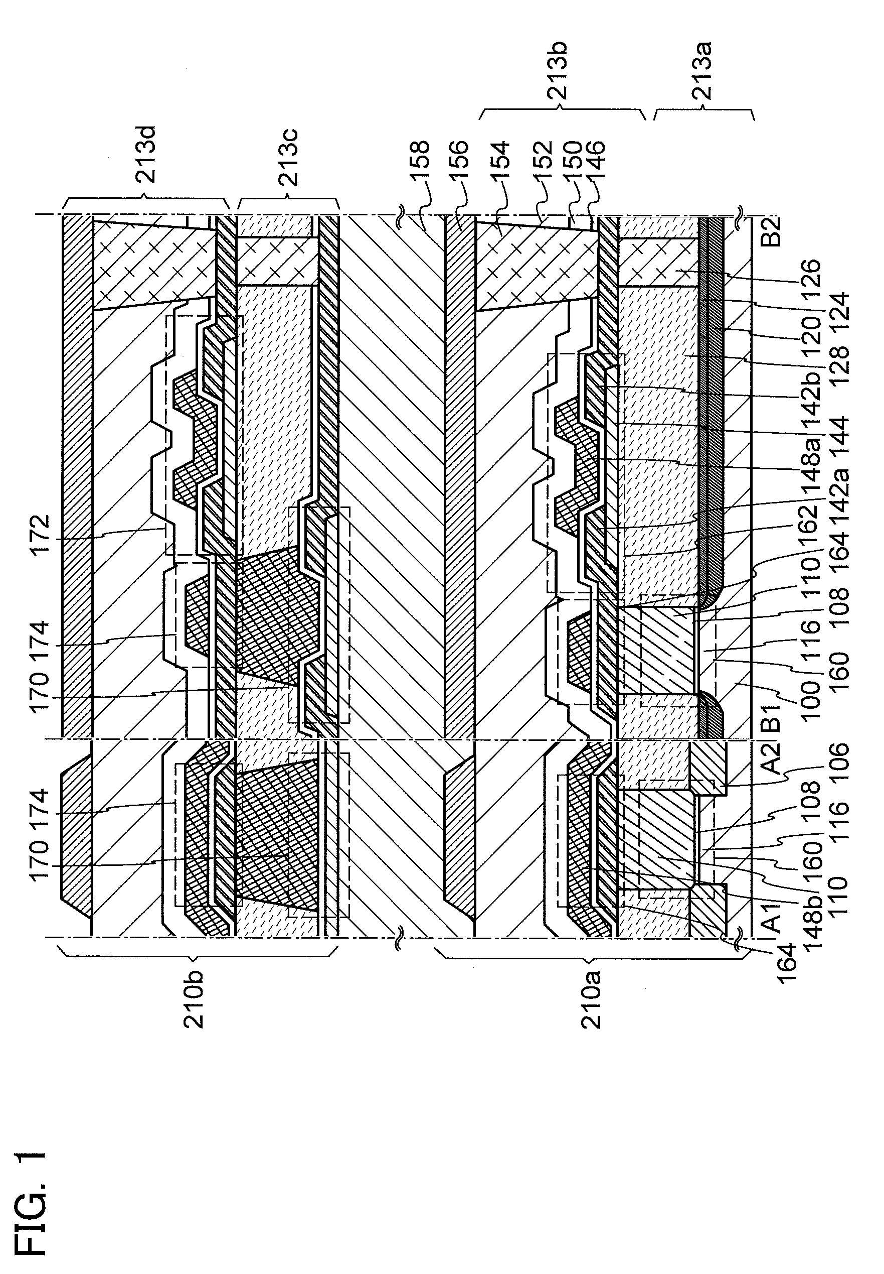
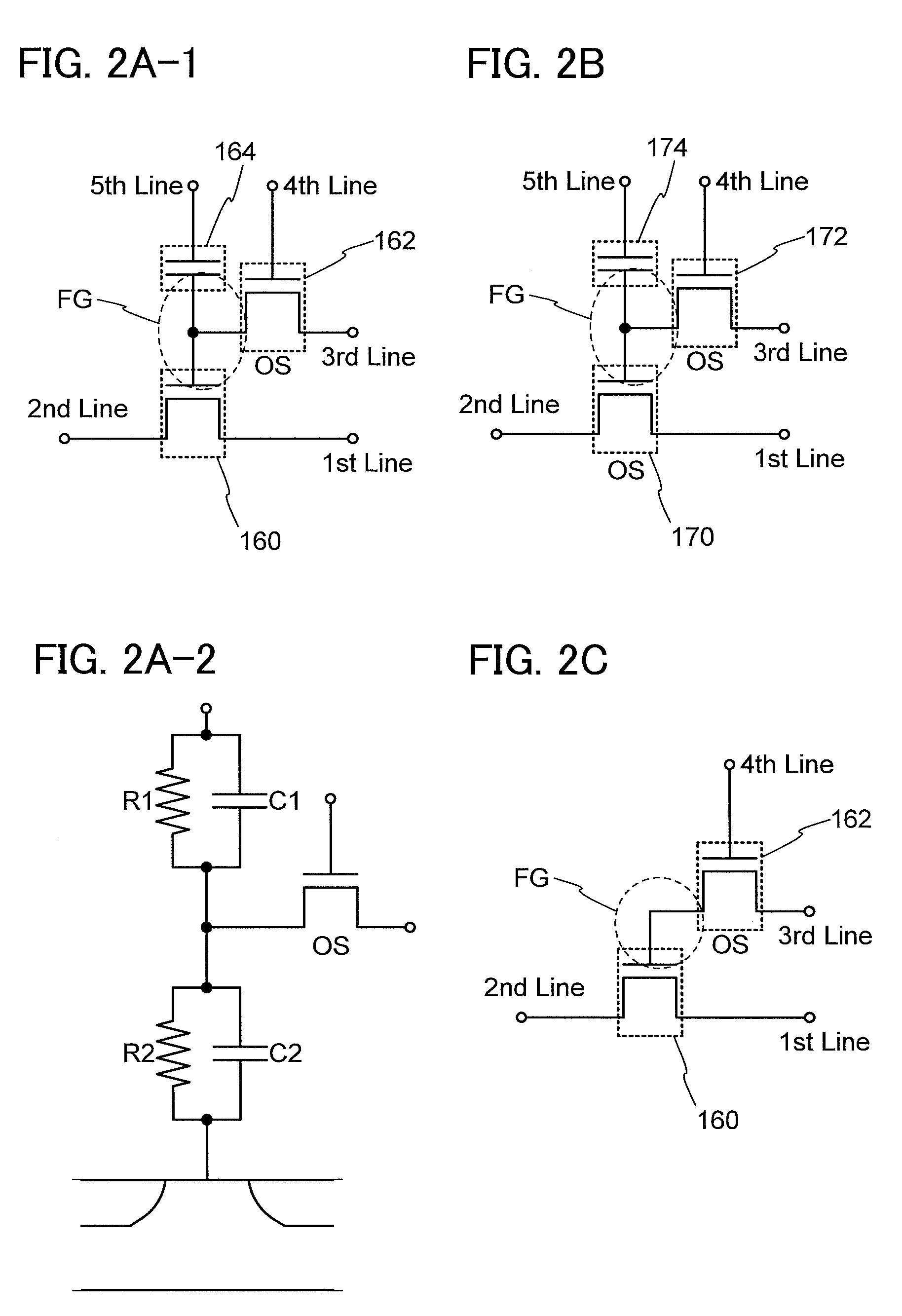
[0053]In this embodiment, a structure and a manufacturing method of a semiconductor device according to one embodiment of the present invention will be described with reference to FIG. 1, FIGS. 2A-1, 2A-2, 2B, and 2C, FIG. 3, FIG. 4, FIG. 5, FIG. 6, FIG. 7, FIG. 8, FIG. 9, FIG. 10, FIG. 11, FIG. 12, FIG. 13, FIG. 14, FIG. 15, FIGS. 16A to 16D, FIGS. 17A to 17D, FIGS. 18A to 18D, and FIGS. 19A and 19B.

[0054]FIG. 1 illustrates a cross section of a semiconductor device. In FIG. 1, A1-A2 is a cross section perpendicular to a channel length direction of a transistor, and B1-B2 is a cross section parallel to the channel length direction of the transistor. The semiconductor device illustrated in FIG. 1 includes a first stack 210a and a second stack 210b. In the first stack 210a, a transistor 160 including a first semiconductor material is provided in a lower portion, and a transistor 162 including a second semiconductor material is provided in an upper portion. In the second stack 210b, a ...

embodiment 2

[0212]In this embodiment, application of the semiconductor device described in the above embodiment to an electronic device will be described with reference to FIGS. 20A to 20F. In this embodiment, examples of the electronic device to which the above semiconductor device is applied include a computer, a mobile phone (also referred to as a cellular phone or a mobile phone device), a portable information terminal (including a portable game machine, an audio reproducing device, and the like), a camera such as a digital camera or a digital video camera, electronic paper, and a television device (also referred to as a television or a television receiver).

[0213]FIG. 20A illustrates a laptop computer including a housing 701, a housing 702, a display portion 703, a keyboard 704, and the like. A memory circuit is provided inside at least one of the housings 701 and 702, and the memory circuit includes the semiconductor device described in the above embodiment. Therefore, a laptop computer in...


PUM


Abstract

An object is to provide a semiconductor device with a novel structure in which stored data can be held even when power is not supplied and there is no limit on the number of write operations. The semiconductor device includes a first memory cell including a first transistor and a second transistor, a second memory cell including a third transistor and a fourth transistor, and a driver circuit. The first transistor and the second transistor overlap at least partly with each other. The third transistor and the fourth transistor overlap at least partly with each other. The second memory cell is provided over the first memory cell. The first transistor includes a first semiconductor material. The second transistor, the third transistor, and the fourth transistor include a second semiconductor material.

Description

TECHNICAL FIELD[0001]The present invention relates to a semiconductor device using a semiconductor element and a method for manufacturing the semiconductor device.BACKGROUND ART[0002]Memory devices using semiconductor elements are broadly classified into two categories: a volatile device that loses stored data when power supply stops, and a nonvolatile device that holds stored data even when power is not supplied.[0003]A typical example of a volatile memory device is a dynamic random access memory (DRAM). A DRAM stores data in such a manner that a transistor included in a memory element is selected and charge is stored in a capacitor.[0004]When data is read from a DRAM, charge in a capacitor is lost according to the above principle; thus, another write operation is necessary every time data is read. Moreover, a transistor included in a memory element has leakage current (off-state current) between a source and a drain in an off state, or the like and charge flows into or out of a ca...

Claims


Application Information

Patent Timeline
Patent Type & Authority Patents(United States)
IPC IPC(8): H01L27/108
CPCH01L27/0688H01L27/1052H01L27/11551H01L27/1156H01L27/1203H01L27/10805H01L27/11521G11C16/0433G11C16/08G11C16/10G11C16/26H10B41/30H10B41/70H10B41/20H10B99/00H10B12/30H10B99/22
Inventor KATO, KIYOSHI
Owner SEMICON ENERGY LAB CO LTD
Why Eureka
Try Eureka