Semiconductor device and manufacturing method thereof

a semiconductor device and manufacturing method technology, applied in the direction of semiconductor devices, basic electric elements, electrical appliances, etc., can solve the problems of increasing power consumption of semiconductor devices, difficult to ensure an adequate period of charge retention, and hardly be said, and achieve novel structure, excellent characteristics, and improved characteristics of transistors including oxide semiconductors

Active Publication Date: 2013-03-05
SEMICON ENERGY LAB CO LTD
View PDF132 Cites 63 Cited by
  • Summary
  • Abstract
  • Description
  • Claims
  • Application Information

AI Technical Summary

Benefits of technology

[0022]With a structure in which a transistor including an oxide semiconductor and a transistor including a material other than an oxide semiconductor are stacked, a semiconductor device having advantages of both of the transistors can be provided. In particular, with respect to a transistor including an oxide semiconductor, which has a source electrode and a drain electrode with an oxidized side surface, characteristics such as subthreshold swing (S-value), on / off ratio, and reliability are significantly improved. Specifically, the following structure can be employed, for example.
[0042]In particular, the off-state current of a transistor including an oxide semiconductor is extremely small and the switching characteristic thereof is excellent; thus, an excellent semiconductor device can be provided utilizing the characteristics. A transistor including a material other than an oxide semiconductor is advantageous over a transistor including an oxide semiconductor in terms of field-effect mobility and the like, and this can be utilized to provide a semiconductor device taking advantage of the characteristics. In other words, according to an embodiment of the present invention, an excellent semiconductor device having characteristics of both an oxide semiconductor and a material other than an oxide semiconductor can be provided.
[0044]In addition, according to an embodiment of the disclosed invention, characteristics of a transistor including an oxide semiconductor are further improved by supplying oxygen to an oxide semiconductor layer. Here, the oxygen supply process brings the result that a side surface of a source or drain electrode is oxidized in a transistor including an oxide semiconductor.
[0045]By oxidizing a side surface of a source or drain electrode, it is possible to prevent short circuit between a gate electrode and the source or drain electrode which may be caused by a reduction in thickness of a gate insulating layer or defective coverage therewith.
[0046]By supplying oxygen to an oxide semiconductor layer as described above, a semiconductor device with a novel structure and excellent characteristics can be realized.

Problems solved by technology

However, it can hardly be said that even a semiconductor device for which silicon or the like is used as a material has sufficient characteristics for some applications.
Therefore, a slight amount of current flows regardless of the operation state of the semiconductor device, and thus it has been difficult to ensure an adequate period for charge retention in the case of fabrication of a charge-retention semiconductor device such as a memory device or a liquid crystal display device.
In addition, there is a problem in that the power consumption of the semiconductor device increases due to the off-state current.

Method used


Image

  • Semiconductor device and manufacturing method thereof
  • Semiconductor device and manufacturing method thereof
  • Semiconductor device and manufacturing method thereof

Examples


embodiment 1

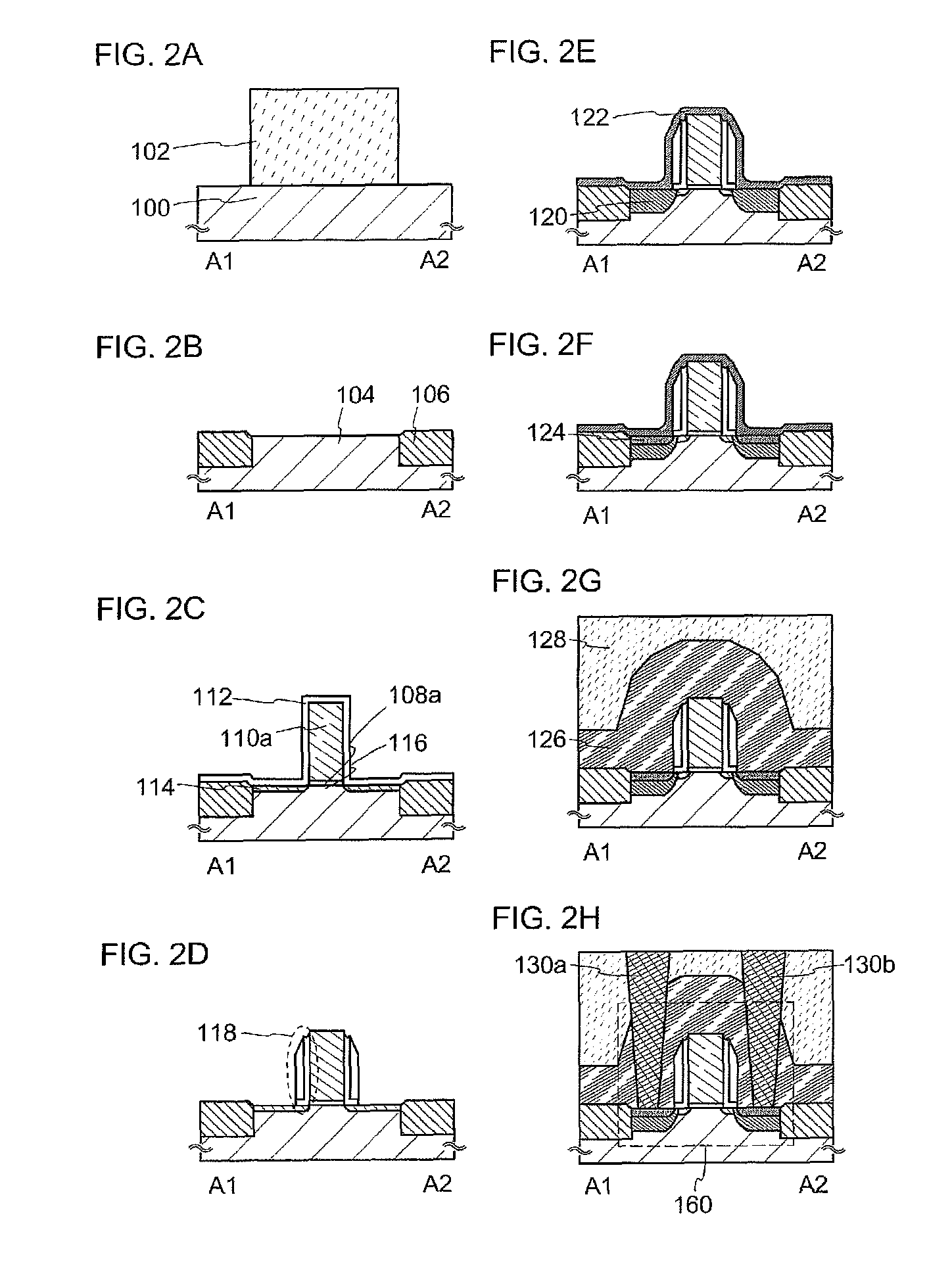
[0068]In this embodiment, a structure and a manufacturing method of a semiconductor device according to one embodiment of the disclosed invention will be described with reference to FIGS. 1A and 1B, FIGS. 2A to 2H, FIGS. 3A to 3E, and FIGS. 4A to 4D.

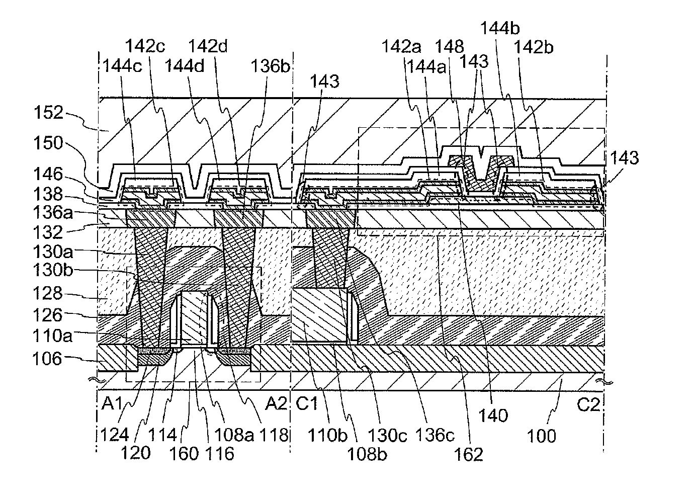
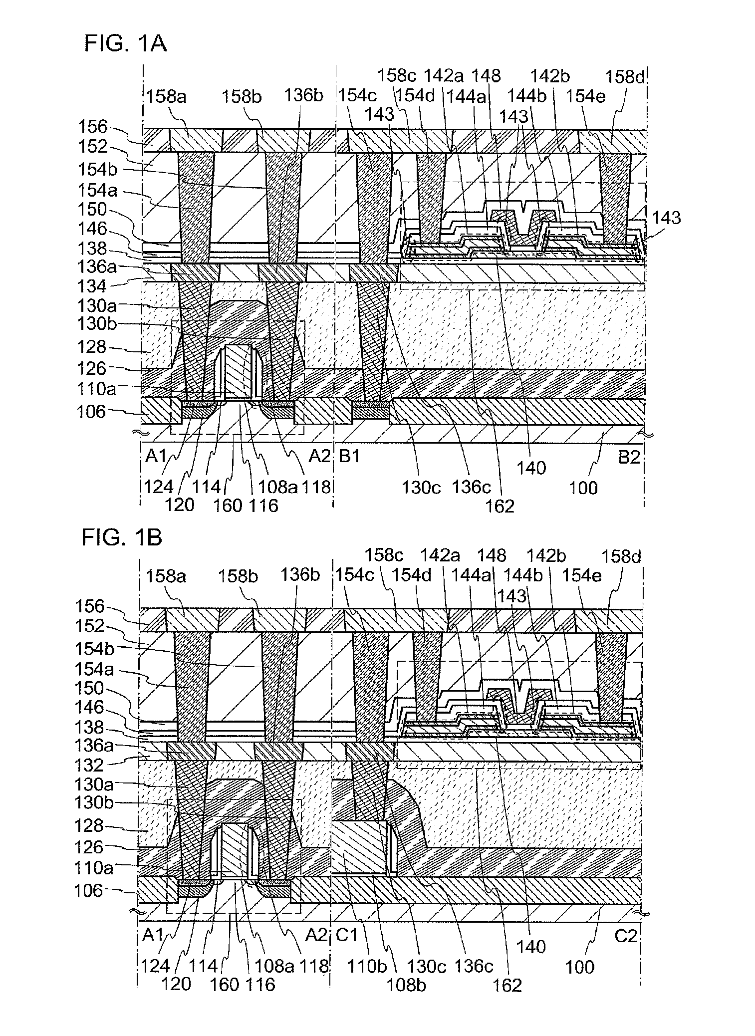
[0069]FIGS. 1A and 1B are cross-sectional views each illustrating an example of a structure of a semiconductor device. The semiconductor device illustrated in FIG. 1A includes, in a lower portion, a transistor 160 including a material other than an oxide semiconductor, and in an upper portion, a transistor 162 including an oxide semiconductor. The transistors 160 and 162 are n-channel transistors here; alternatively, a p-channel transistor may be used. In particular, it is easy to use a p-channel transistor as the transistor 160. FIG. 1B illustrates an example where the connection relationship between the transistor 162 and an electrode (or a wiring) in the lower portion differs from that in FIG. 1A. The structure in FIG. 1A is mainly de...

embodiment 2

[0216]In this embodiment, a modified example of the semiconductor device described in the above embodiment will be described with reference to FIGS. 16A and 16B.

[0217]FIGS. 16A and 16B are cross-sectional views each illustrating an example of a structure of a semiconductor device. The semiconductor device illustrated in FIG. 16A includes, in a lower portion, a transistor 160 including a material other than an oxide semiconductor, and in an upper portion, a transistor 162 including an oxide semiconductor. Note that the structure of the transistor 160 is similar to that of the transistor 160 described in the above embodiment. FIG. 16B illustrates an example where the connection relationship between the transistor 162 and an electrode (or a wiring) in the lower portion differs from that in FIG. 16A. The structure in FIG. 16A is mainly described below. Note that FIG. 16A shows a cross-sectional view of the transistor 160 provided in the lower portion along A1-A2 and a cross-sectional vi...

embodiment 3

[0225]In this embodiment, examples of electronic devices each including the semiconductor device according to any of the above-described embodiments will be described with reference to FIGS. 17A to 17F. The semiconductor device according to any of the above embodiments has unprecedented excellent characteristics. Therefore, an electronic device with a novel structure can be provided by using the semiconductor device. Note that the semiconductor device according to any of the above embodiments is integrated and mounted on a circuit board or the like, and incorporated in an electronic device.

[0226]FIG. 17A illustrates a notebook personal computer including the semiconductor device according to any of the above embodiments, and includes a main body 301, a housing 302, a display portion 303, a keyboard 304, and the like. By applying the semiconductor device according to the disclosed invention to a personal computer, a high-performance personal computer can be provided.

[0227]FIG. 17B il...


PUM


Abstract

An object is to provide a semiconductor device with a novel structure. A semiconductor device includes a first transistor, which includes a channel formation region provided in a substrate including a semiconductor material, impurity regions, a first gate insulating layer, a first gate electrode, and a first source electrode and a first drain electrode, and a second transistor, which includes an oxide semiconductor layer over the substrate including the semiconductor material, a second source electrode and a second drain electrode, a second gate insulating layer, and a second gate electrode. The second source electrode and the second drain electrode include an oxide region formed by oxidizing a side surface thereof, and at least one of the first gate electrode, the first source electrode, and the first drain electrode is electrically connected to at least one of the second gate electrode, the second source electrode, and the second drain electrode.

Description

TECHNICAL FIELD[0001]A technical field of the present invention relates to a semiconductor device and a manufacturing method of the semiconductor device. Note that semiconductor devices herein refer to general elements and devices which function by utilizing semiconductor characteristics.BACKGROUND ART[0002]There are a wide variety of metal oxides and such material oxides are used for various applications. Indium oxide is a well-known material and is used as a material for transparent electrodes which are needed for liquid crystal display devices or the like.[0003]Some metal oxides have semiconductor characteristics. Examples of such metal oxides having semiconductor characteristics include tungsten oxide, tin oxide, indium oxide, zinc oxide, and the like. A thin film transistor in which a channel formation region is formed using such a metal oxide is already known (see, for example, Patent Documents 1 to 4, Non-Patent Document 1, and the like).[0004]Not only single-component oxides...

Claims


Application Information

Patent Timeline
Patent Type & Authority Patents(United States)
IPC IPC(8): H01L21/302H01L21/461
CPCH01L21/8221H01L27/0688H01L27/1207H01L29/24H01L27/1225
Inventor YAMAZAKI, SHUNPEIKOYAMA, JUN
Owner SEMICON ENERGY LAB CO LTD
Why Eureka
Try Eureka