Semiconductor device having gate trenches and manufacturing method thereof

a technology of semiconductor devices and gate trenches, which is applied in the direction of semiconductor devices, basic electric elements, electrical appliances, etc., can solve the problems of difficult to form fine patterns by photolithography and dry etching, limited photolithographic and dry etching targets, and significant increase in contact resistance, so as to prevent the reduction of active region patterns, suppress the reduction of diffusion layers, and easy to resolve

Active Publication Date: 2013-03-05
LONGITUDE LICENSING LTD
View PDF8 Cites 4 Cited by
  • Summary
  • Abstract
  • Description
  • Claims
  • Application Information

AI Technical Summary

Benefits of technology

[0014]According to the present invention, the STI region does not isolate and separate the first transistor from the second transistor. Instead, the dummy gate trench is provided in the active region where the first and second gate electrodes are formed, the dummy gate electrode is formed in the dummy gate trench, and the dummy gate electrode is arranged between the diffusion layer of the first transistor and the diffusion layer of the second transistor. The dummy gate electrode thereby functions as an element isolation region. Therefore, photolithographic and dry etching targets can be limited to line-and-space patterns extending in the first direction. The line-and-space patterns are relatively easy to resolve by the photolithography. Therefore, it is possible to prevent reduction in active region patterns in the first direction. Accordingly, it is possible to suppress reduction in areas of the diffusion layers and suppress a contact area between the contact plug and one diffusion layer from being reduced. This can suppress contact resistance to be sufficiently low.

Problems solved by technology

However, along with downscaling of semiconductor devices, it has been difficult to form fine patterns by photolithography and dry etching.
For example, the following problems occur when the active regions surrounded by the STI regions in a region where memory cells are formed to have minimum working dimensions such as a memory cell region of a DRAM.
Accordingly, there occurs a problem that contact resistance considerably increases.
While problems of conventional techniques have been described while referring to a memory cell region of a DRAM by way of example, these problems similarly and possibly occur to peripheral regions of a DRAM and in formation of fine patterns in other semiconductor devices.
Therefore, photolithographic and dry etching targets can be limited to line-and-space patterns extending in the first direction.

Method used


Image

  • Semiconductor device having gate trenches and manufacturing method thereof
  • Semiconductor device having gate trenches and manufacturing method thereof
  • Semiconductor device having gate trenches and manufacturing method thereof

Examples


first embodiment

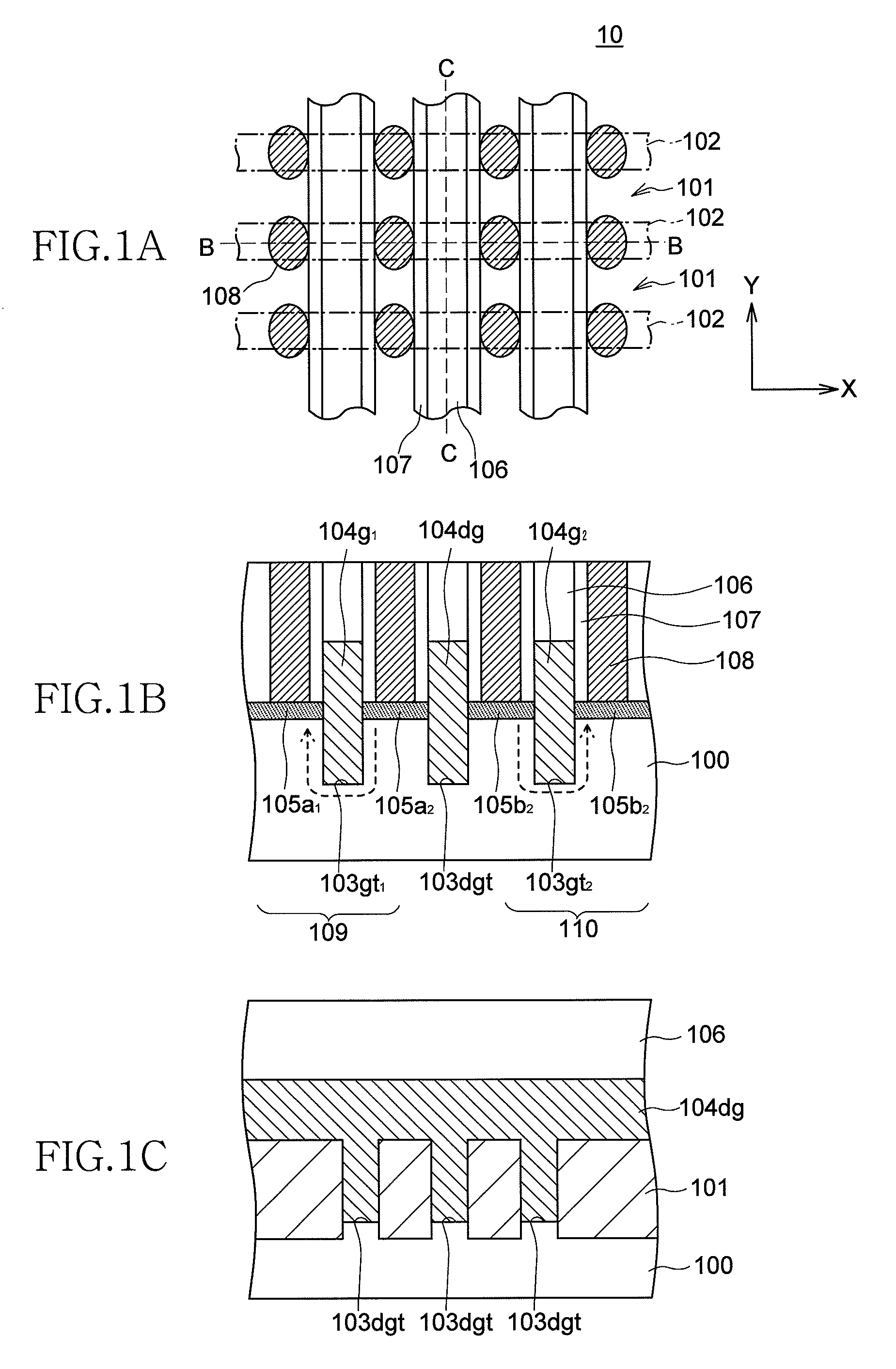
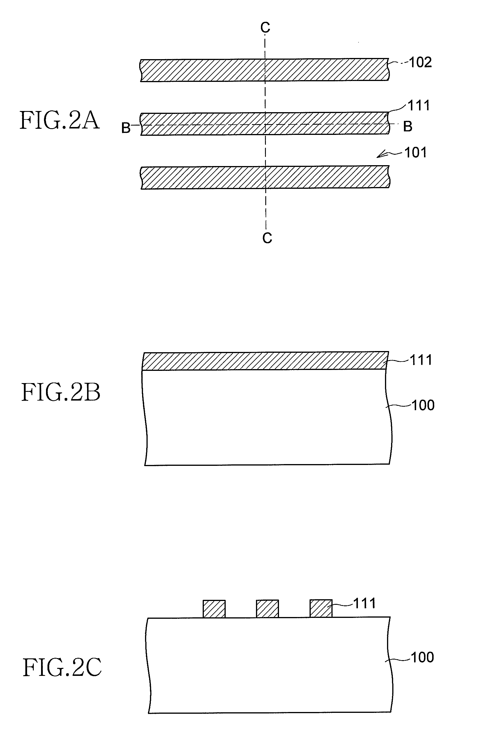
[0045]As shown in FIGS. 1A to 1C, the semiconductor device 10 is configured to include active regions 102 provided in a semiconductor substrate 100, defined and divided by STI regions 101, and extending in an X direction (a first direction), first gate trenches 103gt1, second gate trenches 103gt2, and dummy gate trenches 103dgt provided in the active regions 102, and first gate electrodes 104g1, second gate electrodes 104g2, and dummy gate electrodes 104dg which extend in a Y direction (second direction) crossing the active regions 102, and at least a part of which are buried in the first gate trenches 103gt1, second gate trenches 103gt2, and dummy gate trenches 103dgt, respectively. Each of the dummy gate electrodes 104dg is arranged between one first gate electrode 104g1 and one second gate electrode 104g2.

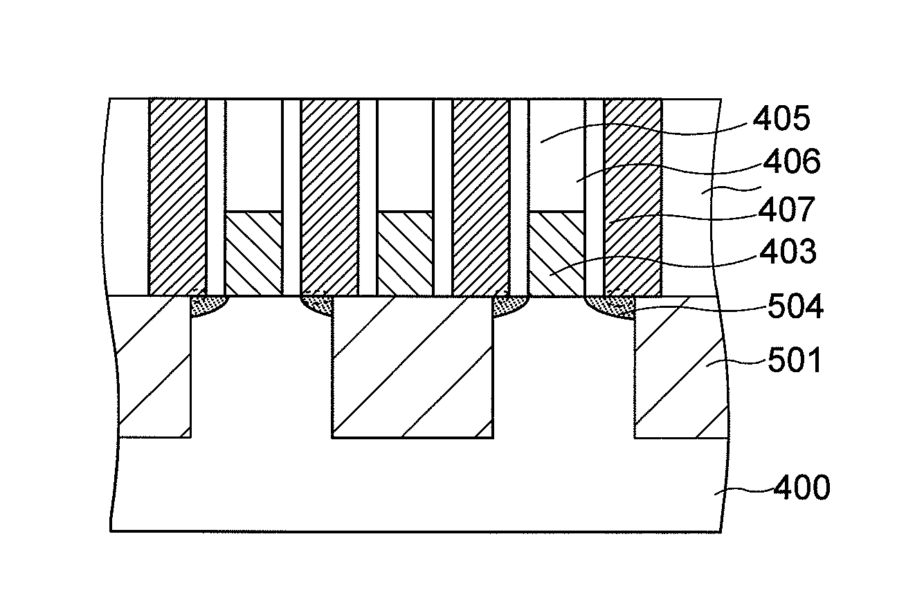
[0046]First to fourth diffusion layers 105a1, 105a2, 105b1, and 105b2 to serve as source / drain regions are provided on both sides of the first and second gate electrodes 104g1 ...

second embodiment

[0058]As shown in FIG. 7D, the semiconductor device 20 includes fin portions 211 provided in lower portions of side surfaces of first and second gate trenches 203gt1 and 203gt2 in an X direction, formed by a part of a semiconductor substrate 200, and constituting a part of channel regions, respectively. Regions defined and divided by STI regions 201 and each indicated by a one-dot chain line are active regions 202. In a first transistor 209 and a second transistor 210, channel regions formed when a predetermined bias is applied to each of first and second gate electrodes 204gt1 and 204gt2 are formed not only on side surfaces and bottom surfaces of the first and second gate trenches 203gt1 and 203gt2 in a Y direction but also on the fin portions 211 provided on the side surfaces thereof in the X direction. By this arrangement, it is possible to reduce threshold voltages of the first and second transistors 209 and 210. Meanwhile, as shown in FIG. 7C, no fin portions are formed on sid...

third embodiment

[0074]A manufacturing method of the semiconductor device 30 is described next.

[0075]FIGS. 18A to 18D to FIGS. 25A to 25D show manufacturing processes of the manufacturing method of the semiconductor device 30 according to the third embodiment. In FIGS. 18A to 18D to FIGS. 25A to 25D, each drawing tagged as “A” is a schematic plan view, each drawing tagged as “B” is a schematic cross-sectional view taken along a line B-B of “A”, each drawing tagged as “C” is a schematic cross-sectional view taken along a line C-C of “A”, and each drawing tagged as “D” is a schematic cross-sectional view taken along a line D-D of “A”. When the schematic cross-sectional view taken along the line D-D is identical to that taken along the line C-C, the drawing tagged as “D” will be omitted.

[0076]First, as shown in FIGS. 19A to 19D, a first mask layer 313 having line-and-space patterns is formed on the semiconductor substrate 300. The region indicated by a one-dot chain line is to serve as the active regi...


PUM


Abstract

A semiconductor device includes a first gate trench, a second gate trench, and a dummy gate trench provided in an active region extending in an X direction; and a first gate electrode, a second gate electrode, and a dummy gate electrode extending in a Y direction crossing the active region, at least a part of which are buried in the first gate trench, the second gate trench, and the dummy gate trench, respectively. The dummy gate electrode arranged between second and third diffusion layers isolates and separates a transistor constituted by the first gate electrode and first and second diffusion layers provided on both sides of the first gate electrode, respectively, from a transistor constituted by the second gate electrode and third and fourth diffusion layers provided on both sides of the second gate electrode, respectively.

Description

BACKGROUND OF THE INVENTION[0001]1. Field of the Invention[0002]The present invention relates to a semiconductor device and a manufacturing method thereof, and more particularly relates to a semiconductor device including trench gate transistors (trench gate is also referred to as “recess channel”, see Japanese Patent Application Laid-open Nos. 2005-322880, 2006-173429, and 2006-261627) and a manufacturing method of the semiconductor device.[0003]2. Description of Related Art[0004]Generally, in a manufacturing method of a semiconductor device, fine patterns are formed by photolithography and dry etching.[0005]FIGS. 26A and 26B show a configuration of memory cell transistors of an ordinary DRAM, where FIG. 26A is a schematic plan view and FIG. 26B is a schematic cross-sectional view taken along a line B-B of FIG. 26A.[0006]As shown in FIGS. 26A and 26B, STI (Shallow Trench Isolation) regions 401 are formed in a semiconductor substrate 400 by photolithography and dry etching, thereby ...

Claims


Application Information

Patent Timeline
Patent Type & Authority Patents(United States)
IPC IPC(8): H01L29/78
CPCH01L29/66795H01L29/785
Inventor MIKASA, NORIAKI
Owner LONGITUDE LICENSING LTD
Why Eureka
Try Eureka