
Graphene optical sensor

a graphene optical sensor and optical sensor technology, applied in the field of optical sensors, can solve the problems of not having the idealized flat geometry of graphene films, affecting the formation of curved structures such as soot, fullerenes, nanotubes or buckles,

Active Publication Date: 2013-03-12
INT BUSINESS MASCH CORP +1
View PDF17 Cites 19 Cited by
  • Summary
  • Abstract
  • Description
  • Claims
  • Application Information

AI Technical Summary

Benefits of technology

The graphene optical sensor effectively determines the composition of analytes by identifying shifts in the optical absorption spectrum, enabling applications in chemical, environmental, and biosensing, with the ability to analyze multiple analytes simultaneously and adjust sensitivity through doping or plasma exposure.

Problems solved by technology

A free-standing graphene structure is theoretically stable only in a two-dimensional space, which implies that a truly planar graphene structure does not exist in a three-dimensional space, being unstable with respect to formation of curved structures such as soot, fullerenes, nanotubes or buckled two dimensional structures.
Free standing graphene films have also been produced, but they may not have the idealized flat geometry.
However, by subjecting the bi-layer graphene to an electric field, a charge imbalance can be induced between the two layers, and this will lead to a different band structure with a band gap proportional to the charge imbalance.

Method used


Image

  • Graphene optical sensor
  • Graphene optical sensor
  • Graphene optical sensor

Examples


Embodiment Construction

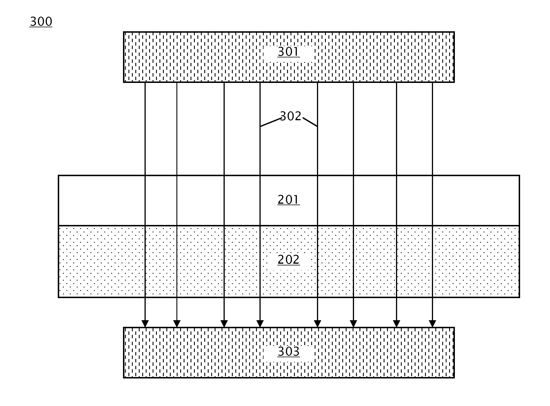
[0017]Embodiments of a graphene optical sensor and methods of using a graphene optical sensor are provided, with exemplary embodiments being discussed below in detail. Operation of an optical sensor may be based on detection of a shift in a peak resonance frequency of surface plasmons (i.e., collective oscillations of electrons) on a sensing surface in the presence of an analyte. Surface plasmons may be excited on a sensing surface, which may include a noble metal such as silver or gold, using polarized light in total internal reflection (TIR) mode. The peak plasmon resonance of the sensing surface may be observed by measuring the optical absorption spectrum of the sensing surface using a spectrophotometer. Graphene is a semi-metal material on which surface plasmons may be excited, and is also transparent. Therefore, an optical sensor that utilizes graphene as the sensing surface may be used in both TIR and transmission mode, unlike an optical sensor that uses a metal for the sensin...


PUM

PropertyMeasurementUnit
stacking distanceaaaaaaaaaa
peak wavelengthaaaaaaaaaa
optical absorption spectrumaaaaaaaaaa

Abstract

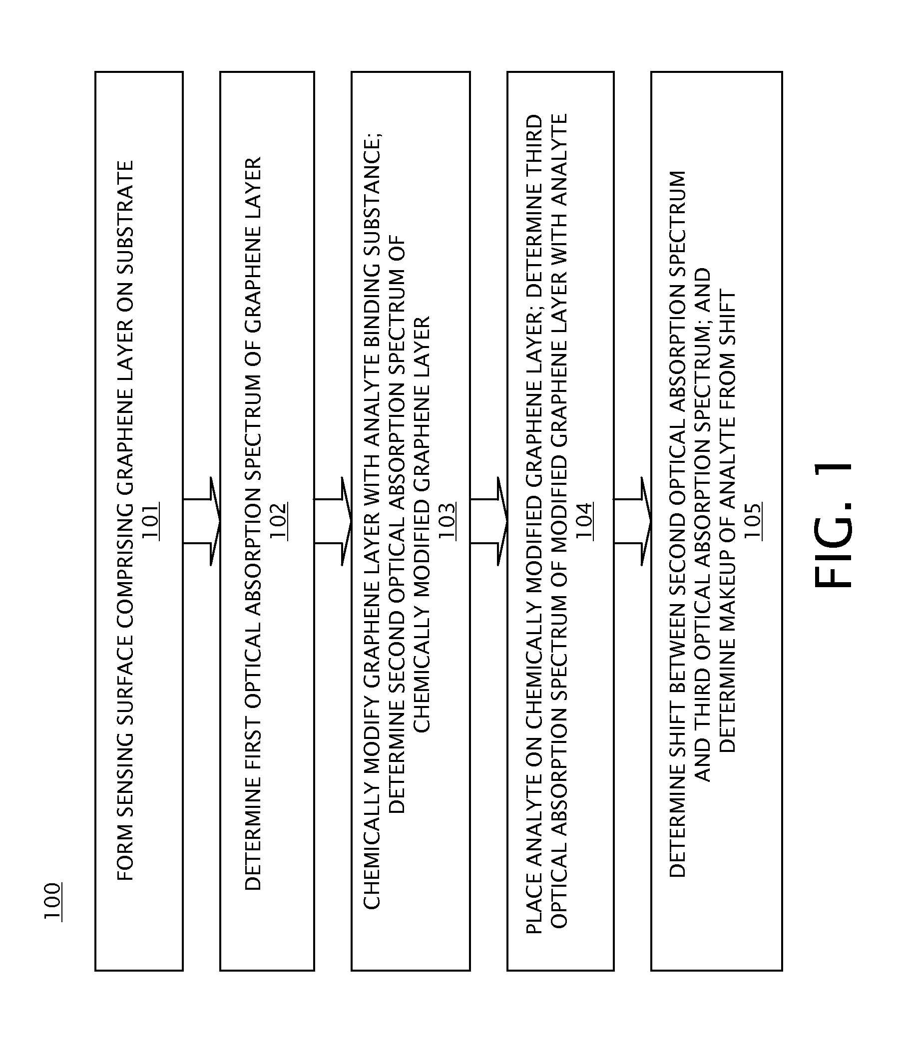
A method of using an optical sensor, the optical sensor comprising a sensing surface comprising graphene layer, the sensing surface located on a substrate, includes determining a first optical absorption spectrum for the graphene layer by a spectrophotometer; adding an analyte, the analyte selected to cause a shift in the first optical absorption spectrum, to the graphene layer; determining a second optical absorption spectrum for the modified graphene layer by a spectrophotometer; determining a shift between the first optical absorption spectrum and the second optical absorption spectrum; and determining a makeup of the analyte based on the determined shift.

Description

FIELD[0001]This disclosure relates generally to the field of optical sensors, and more particularly to a graphene optical sensor.DESCRIPTION OF RELATED ART[0002]Graphene refers to a two-dimensional planar sheet of carbon atoms arranged in a hexagonal benzene-ring structure. A free-standing graphene structure is theoretically stable only in a two-dimensional space, which implies that a truly planar graphene structure does not exist in a three-dimensional space, being unstable with respect to formation of curved structures such as soot, fullerenes, nanotubes or buckled two dimensional structures. However, a two-dimensional graphene structure may be stable when supported on a substrate, for example, on the surface of a silicon carbide (SiC) crystal. Free standing graphene films have also been produced, but they may not have the idealized flat geometry.[0003]Structurally, graphene has hybrid orbitals formed by sp2 hybridization. In the sp2 hybridization, the 2s orbital and two of the th...

Claims


Application Information

Patent Timeline
Patent Type & Authority Patents(United States)
IPC IPC(8): G01N21/00G01J3/42
CPCG01N21/553G01N21/77G01N2021/7773G01N2021/7783
Inventor AFZALI, ALIBOL, AGEETH A.KASRY, AMALTULEVSKI, GEORGE S.
Owner INT BUSINESS MASCH CORP
Learn More