Integrated circuit module time delay budgeting

a technology of integrated circuits and time delay, applied in the field of integrated circuit (ic) design, can solve the problems of increasing the complexity of the interconnection system of such ics, increasing the size, complexity, operating or switching speed of semiconductor ics, and reducing the geometries, so as to achieve a high degree of confiden

Active Publication Date: 2013-03-12
AMPERE COMPUTING LLC
View PDF37 Cites 2 Cited by
  • Summary
  • Abstract
  • Description
  • Claims
  • Application Information

AI Technical Summary

Benefits of technology

[0009]Disclosed herein is a method of estimating interface timing paths between modules in an integrated circuit (IC) using expected gate-delays, wire-distances, wire-type, fallout, and other design considerations, based on an early floor-plan. Thereafter, all the interface timing paths (timing budgets) of the modules can be measured at the top-level to make sure they meet the design target. Since the module level timing budgets are made with a high level of confidence, each module can be designed independently. In addition, this approach also enables early micro-architecture validation of the module interfaces

Problems solved by technology

The size, complexity, and operating or switching speeds of semiconductor ICs have increased, while feature geometries have decreased, and interconnect systems for such ICs have dramatically increased in complexity.
While such timing measurements can theoretically be performed using a rigorous circuit simulation, such an approach is liable to be too slow to be practical.
Faster design times are a result of using simplified STA delay models, and a limited consideration of the effects of logical interactions between signals.
One problem with STA is that the analysis can only be performed after the design and layout of a digital circuit.
By then, it may be too late to change the micro-architecture without impacting the design and schedule.

Method used


Image

  • Integrated circuit module time delay budgeting
  • Integrated circuit module time delay budgeting
  • Integrated circuit module time delay budgeting

Examples


Embodiment Construction

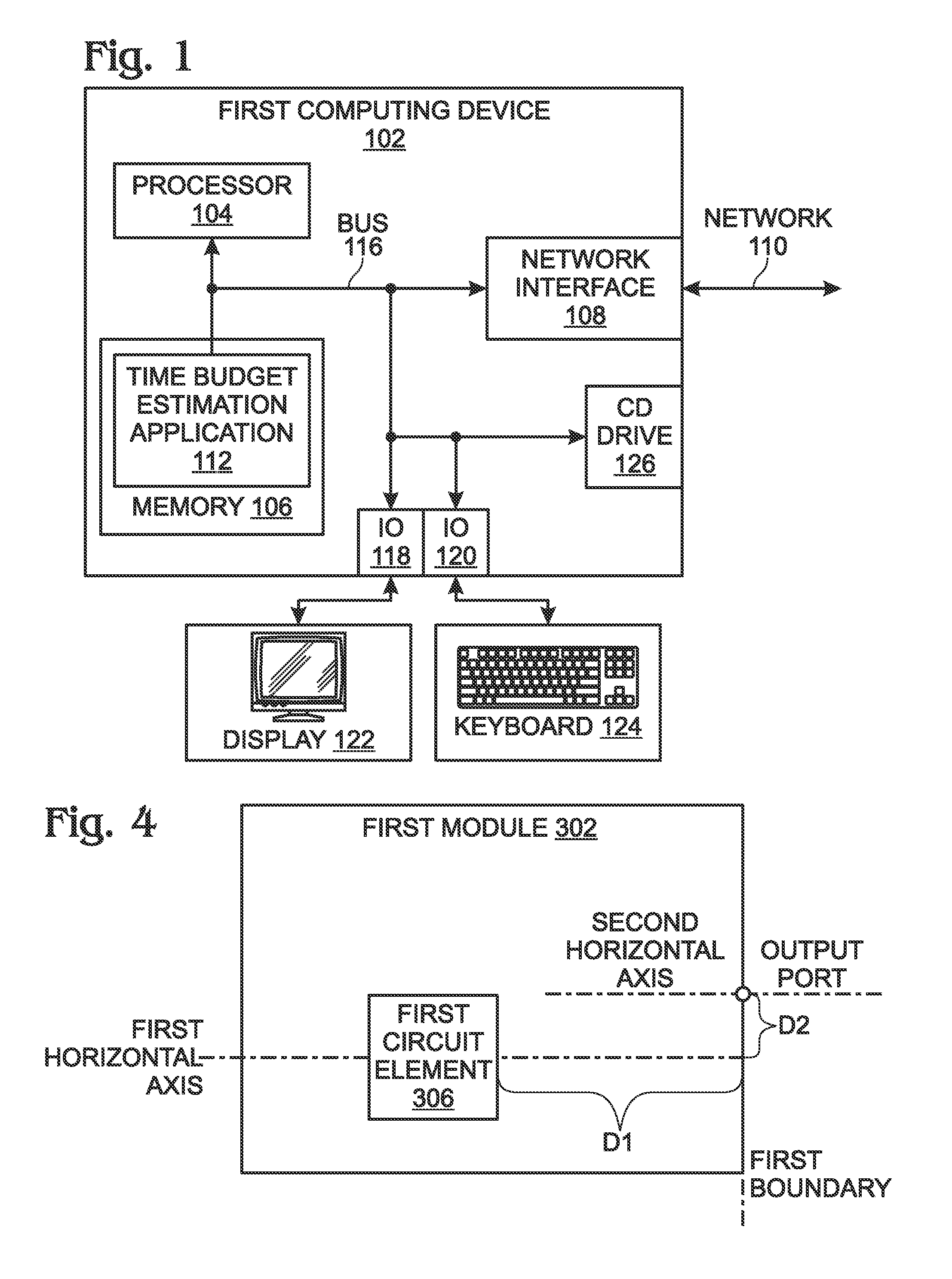
[0033]As used in this application, the terms “component,”“module,”“system,” and the like may be intended to refer to an automated computing system entity, such as hardware, firmware, a combination of hardware and software, software, software stored on a computer-readable medium, or software in execution. For example, a component may be, but is not limited to being, a process running on a processor, a processor, an object, an executable, a thread of execution, a program, and / or a computer. By way of illustration, both an application running on a computing device and the computing device can be a component. One or more components can reside within a process and / or thread of execution and a component may be localized on one computer and / or distributed between two or more computers. In addition, these components can execute from various computer readable media having various data structures stored thereon. The components may communicate by way of local and / or remote processes such as in...


PUM


Abstract

A circuit analysis tool is provided, enabled as computer software instructions, for budgeting time delays between integrated circuit (IC) modules. The instructions accept a command enabling an IC floor-plan including a first module and a second module. The first module includes a first circuit element having a signal output interface, and an output port. The second module includes an input port, and a second circuit element having a signal input interface. A command is accepted defining a maximum delay value, and a first delay value is estimated between the first circuit element signal output interface and the first module output port. A second delay value is estimated between the second circuit element signal input interface and the second module input port, and a third delay value is estimated between the first module output port and the second module input port. The first, second, and third delay values are summed, creating a time budget estimate. The time budget estimate is approved if it is less than the maximum delay value.

Description

BACKGROUND OF THE INVENTION[0001]1. Field of the Invention[0002]This invention generally relates to integrated circuit (IC) design and, more particularly, to a method for allocating timing delay budgets across IC modules using gate-delay and wire-distance estimates.[0003]2. Description of the Related Art[0004]The size, complexity, and operating or switching speeds of semiconductor ICs have increased, while feature geometries have decreased, and interconnect systems for such ICs have dramatically increased in complexity. In a digital circuit, data is supposed to move in lockstep, advancing one stage on each tick of the clock signal. This is enforced by synchronizing elements such as flip-flops or latches, which copy their input to their output when instructed to do so by the clock.[0005]As noted in Wikipedia, one approach that is used to analyze timing errors is to model the interconnect system as an arrangement of nets (interconnections between gate outputs and interconnected gate i...

Claims


Application Information

Patent Timeline
Patent Type & Authority Patents(United States)
IPC IPC(8): G06F17/50
CPCG06F17/5081G06F2217/84G06F30/398G06F2119/12
Inventor CHATTERJEE, MITRAJITBADIDA, SANDEEP
Owner AMPERE COMPUTING LLC
Why Eureka
Try Eureka